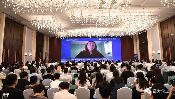
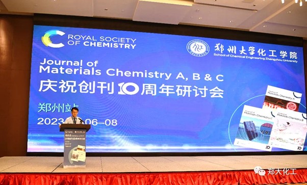
This year we are pleased to celebrate 10 years since Journal of Materials Chemistry was split into three respective journals: Journal of Materials Chemistry A, B and C, each focusing on a different aspect of materials chemistry. We are grateful to our fantastic community of authors, reviewers, Board members and readers and wanted to showcase just some of them in a series of ‘Community Spotlight’ blog articles.
Next in our ‘Community Spotlight’ series, we feature some more of our outstanding peer reviewers who have gone above and beyond in supporting the quality, timely and rigorous peer review model for Journal of Materials Chemistry A, B or C over the years. Check out their interview responses below to find out how reviewing has helped in the preparation of their own manuscripts and to discover their top advice for new reviewers and authors.
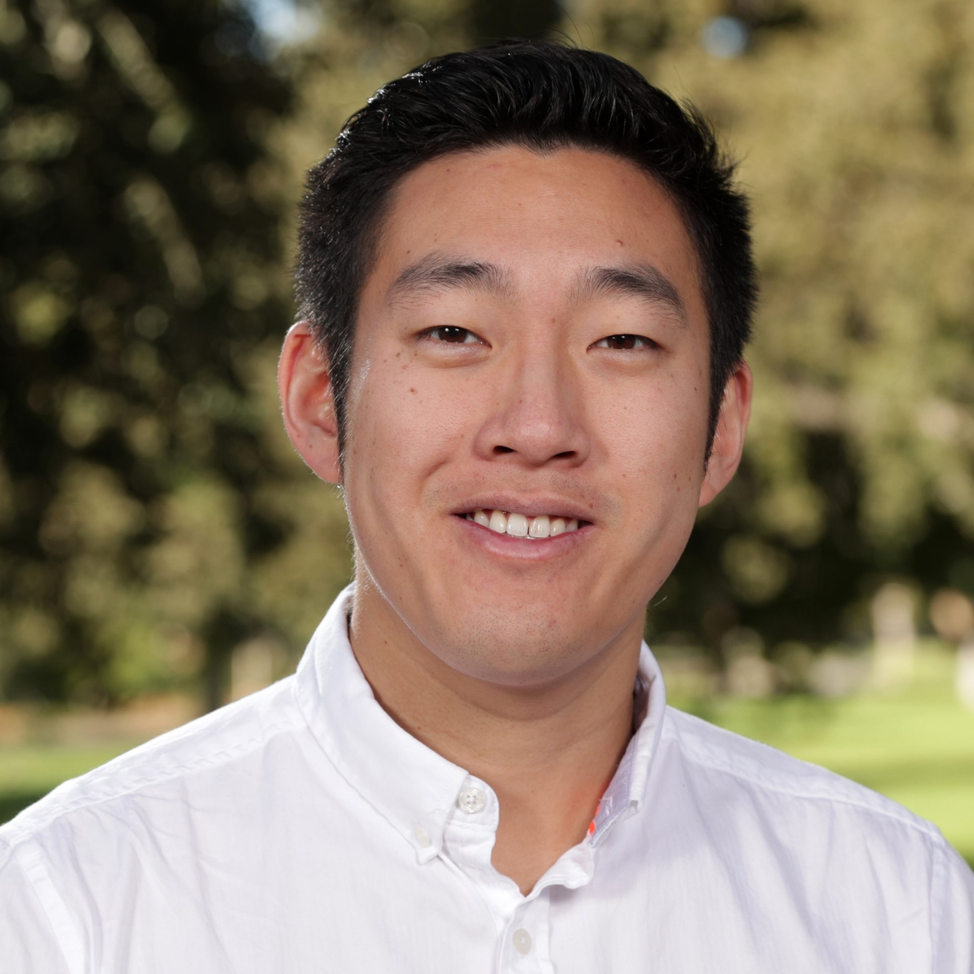
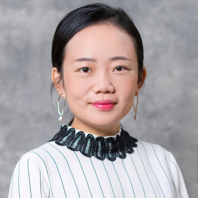
Dr Sijie Chen
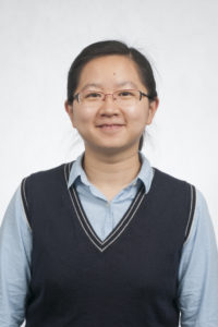
Dr. Sijie Chen received her BSc in Biology from Wuhan University in 2009 and PhD in Bioengineering from Hong Kong University of Science and Technology (HKUST) in 2013, under the supervision of Prof Ben Zhong Tang. She worked as a Postdoctoral Fellow at HKUST and then as an Endeavour Fellow at the University of Melbourne and as a visiting scientist at Walter and Eliza Hall Institute of Medical Research. She joined Prof Ana Teixeira’s group as a Postdoc in the Division of Biomaterials and Regenerative Medicine at the Department of Medical Biochemistry and Biophysics in Karolinska Institutet since late 2015. Dr. Chen was recruited as an Assistant Professor at Ming Wai Lau Centre for Reparative Medicine, Karolinska Institutet in 2017. She will be moving to the Chinese University of Hong Kong (CUHK) this year.
Dr. Chen is working on fluorescent sensors and fluorescence imaging. Her current research interests focus on the development of new luminescent materials for mechanobiology studies and regenerative medicine studies. |
What encouraged you to become a reviewer for Journal of Materials Chemistry B?
As a researcher who publishes papers every year, I usually receive feedback from 2-5 reviewers for each of my papers. I am grateful for the time and effort that reviewers invest in providing constructive suggestions, which help to improve the quality of our research and ensure that the scientific community runs smoothly. I also have some of my own papers published in the Journal of Materials Chemistry B, which has motivated me to contribute my own knowledge and experience to the journal as a reviewer. I am excited to have the opportunity to give back to the scientific community and contribute to the dissemination of high-quality research.
What would you recommend to new reviewers to ensure their report is helpful?
The primary goal of the review process is to provide authors with constructive feedback that can help them improve their work. When reviewing a manuscript, it is important to consider several key factors. These can include the significance and novelty of the work, the design of the project, the clarity of expression, and any errors that have been identified.In providing feedback, it is helpful to be as specific and detailed as possible. For instance, if you question the novelty of the work, you might provide references or examples to support your concerns. Similarly, if you identify language or writing issues, it can be useful to list specific examples or offer suggestions for improvement.
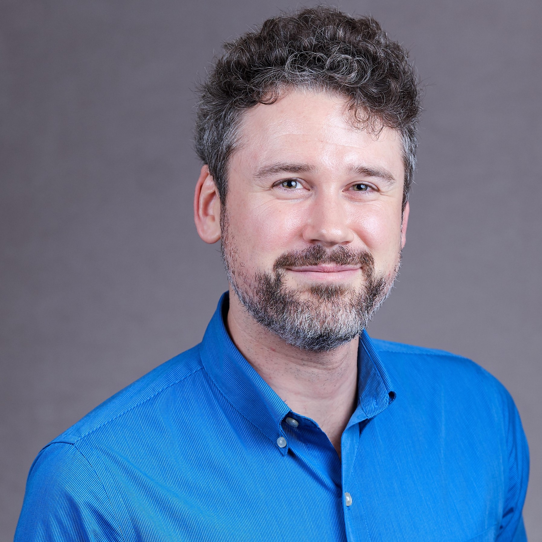
Dr Marcus Johns
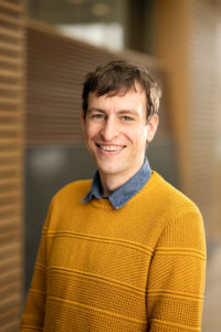
Dr. Marcus Johns is an analytical materials scientist who focuses his research on developing new analytical techniques. These use light to directly investigate the intermolecular structures of polymers and the interparticle interactions of nanomaterials. This research direction emerged from his curiosity about the background fluorescence observed from bio-based scaffolds for tissue engineering. He completed his PhD at the Centre for Sustainable Chemical Technologies, University of Bath, UK in 2017 and is currently a Mitacs Accelerate postdoctoral research fellow in the Faculty of Forestry at the University of British Columbia, Canada. Marcus has been recognized as an outstanding reviewer for the Journal of Materials Chemistry B in both 2020 and 2021. |
What would you recommend to new reviewers to ensure their report is helpful?
My top recommendation is to always provide constructive comments, regardless of your opinion on the manuscript’s quality. If you believe the paper needs significant revisions or should be rejected, explain your reasoning and suggest experiments or alternative theories for the authors to consider. Conversely, even if you initially think that the manuscript is flawless, there may still be areas that need clarification or references that the authors might have missed. Additionally, don’t hesitate to propose new research directions based on the manuscript’s results and your expertise, or ask questions that require further investigation (clarify that you don’t expect answers in the current manuscript). As reviewers, our role extends beyond ensuring scientific soundness; we also support researchers in developing new avenues of inquiry and expanding humanity’s knowledge.
Has being a reviewer affected how you approach the preparation of your recent manuscripts?
Yes, absolutely! First and foremost, I ensure that I prepare the manuscript to the highest possible standard before submission, even if it means taking an extra month. As a reviewer, it becomes challenging to focus solely on the scientific content when the manuscript’s structure is poor or important details are missing. The initial time invested in enhancing the manuscript’s quality is always less than going through multiple review rounds due to confusion or missing information. Similarly, I dedicate time to ensure that the supplementary information for the manuscript includes all relevant data, enabling readers to draw their own conclusions. As a reviewer, there’s nothing more frustrating than being unable to assess the reasonability of a conclusion due to incomplete data. Lastly, I’ve made an effort to educate myself on statistical analysis and ensure its correct application. I often encounter incorrect claims of significance as a reviewer, where the analysis has been repeated but not reproduced, for example.
Professor Jennifer Schaefer

Jennifer L. Schaefer is the Sheehan Family Collegiate Professor of Engineering and the Director of Diversity, Equity, and Inclusion of the Department of Chemical and Biomolecular Engineering at the University of Notre Dame, USA. Her research group investigates materials chemistry phenomena relevant for sustainable technologies, including electrochemical energy storage devices. Prior to joining the University of Notre Dame in 2015, she was a National Research Council Postdoctoral Associate at the National Institute of Standards and Technology. She earned a PhD in chemical engineering at Cornell University, and prior degrees in chemistry and chemical engineering from Widener University. |
What encouraged you to become a reviewer for Journal of Materials Chemistry A?
The peer-reviewed publication system requires both authors and reviewers. As leader of a research group that submits manuscripts, I feel that it is my duty to also review manuscripts. I strive to provide at least the number of manuscript reviews in a given year as a reviewer as I have received as an author. Being a reviewer for manuscripts for non-profit society journals is a way that I serve the global scientific community.
What would you recommend to new reviewers to ensure their report is helpful?
A helpful review considers both the big picture and the details. For manuscripts under review for Journal of Materials Chemistry A, I consider whether the report advances our knowledge of materials chemistry in the application of relevance in light of prior published work. I also look at the details of how the experiments were conducted and compare the displayed data with the claims in the discussion. When claims made in the manuscript do not align with the data presented, then it is constructive to explain in the review exactly what is not aligned. Specific feedback helps authors to more fully understand the reviewer’s perspective and to more quickly identify how to improve their manuscript.
Dr Uroš Lačnjevac

Dr Uroš Lačnjevac is a Full Research Professor at the Institute for Multidisciplinary Research, University of Belgrade, Serbia. He earned his BSc/MSc degree (2005) in electrochemistry from the Faculty of Technology and Metallurgy, University of Belgrade, and his PhD (2010) in energy conversion from the University of Belgrade. His research interests are related to the synthesis of nanostructured materials and composite coatings for electrocatalysis applications, with a focus on water electrolysis. He has published 3 international book chapters and more than 50 papers in peer-reviewed international journals. He has served as a referee for 70 scientific journals and completed more than 430 review reports. For his peer review work, he received the Outstanding Reviewer Award from Journal of Materials Chemistry A in 2019, 2021 and 2022. |
What would you recommend to new reviewers to ensure their report is helpful?
As reviewers, your role is crucial as the bridge between the editor and the authors. It is essential to keep in mind that your responsibility extends in two directions. Firstly, you should assist the editor in making the best decision for the journal’s interests. Secondly, you should help the authors improve their manuscript, irrespective of whether your recommendation is to reject or accept it. When providing your report, strive to be constructive, specific, and comprehensive. This approach demonstrates respect for both the authors and the journal. Remember to maintain a polite tone while remaining firm and persistent in upholding high standards.
Has being a reviewer affected how you approach the preparation of your recent manuscripts?
Being a reviewer, particularly for esteemed journals like Journal of Materials Chemistry A, has had a transformative impact on my approach to manuscript preparation. It represents a pivotal moment for me, especially as I conduct scientific research in a country with its unique set of challenges. Witnessing how my comments, suggestions, and interpretations can significantly enhance the manuscripts of top research groups has instilled a newfound value in my own knowledge and experience. This realization serves as a powerful motivation, boosting my confidence to strive for success in publishing my own work in high-impact journals. Moreover, reviewing the work of other researchers has been a rich source of ideas, feedback, and insights that I now apply to my own projects and writing process. It has made me more mindful of certain aspects, such as clarity, organization, and addressing potential questions or concerns that reviewers may have. Furthermore, experiencing constructive criticism as a reviewer has deepened my appreciation for the importance of thorough revisions and ensuring the overall quality of my own work prior to submission.
Prof. Sheng-Heng Chung
 Highly recommended 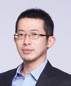 Plan B! |
| Sheng-Heng Chung received his B.S. in Resource Engineering and Materials Science and Engineering from National Cheng Kung University and his M.S. in Materials Science and Engineering from National Tsing Hua University in Taiwan. He joined the Ph.D. program in Materials Science and Engineering and worked as a research associate with Professor Arumugam Manthiram at the University of Texas at Austin. Currently, he is an associate professor in the Department of Materials Science and Engineering at National Cheng Kung University. His current research focuses on electrochemical conversion and storage technology. |
What do you like most about being a reviewer for Journal of Materials Chemistry A?
I have been invited by more than 100 journals and thousands of peer review papers. The peer-review invitation from Journal of Materials Chemistry A always shows high-quality manuscripts with novelty, solid science, and great performance progresses. It is a very nice experience to support these high-standard manuscripts with detailed reviewing and data checking. Moreover, as a reviewer for Journal of Materials Chemistry A, I am always assigned with the papers in my research fields, which means that the authors’ manuscript would be reviewed and polished by researchers in the same and similar research filed. I believe this is important to improve the quality of publications and to help authors.
What encouraged you to become a reviewer for Journal of Materials Chemistry A?
It was a chance that I received a reviewer comment from Journal of Materials Chemistry A, in which the reviewer encourages me to revise my paper with specific suggestions rather than subjective questioning. This encourages me to optimize my reviewer report to a summary with a specific general comment followed by detailed comments supported by my suggestion to address the comment or make improvements. In other words, borrowing from a previous reviewer from Journal of Materials Chemistry A, I believe that the role of a reviewer is to improve the quality of the journal’s publication by offering constructive suggestions for high-level research.
Dr Jianxun Ding
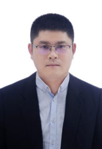
Dr. Jianxun Ding is a professor at Changchun Institute of Applied Chemistry, Chinese Academy of Sciences (CIAC, CAS), P. R. China. Dr. Ding received his B.S. degree from University of Science and Technology of China in 2007 and obtained his Ph.D. at CIAC, CAS, in 2013 under the supervision of Dr. Xuesi Chen. From 2017 to 2019, Dr. Ding worked as a Postdoctoral Research Fellow with Dr. Omid C. Farokhzad and Dr. Jinjun Shi from Brigham and Women’s Hospital, Harvard Medical School. His research focuses on synthesizing biodegradable bioactive polymers, developing bioresponsive polymer platforms for controlled drug delivery, exploiting polymer-based adjuvants for immunotherapy, and preparing polymer scaffolds for regenerative medicine. Dr. Ding has published more than 150 academic articles in mainstream journals, including Advanced Materials, Angewandte Chemie International Edition, and so forth, with over 13,000 citations. Moreover, Dr. Ding has applied for over 70 patents in China, of which over 60 have been authorized. Meanwhile, owing to his significant accomplishments, Dr. Ding has won more than 10 awards, such as the Natural Science Award of Jilin Province, the Science and Technology Progress Award of Jilin Province, the Chinese Chemical Society Polymer Young Scholar Award, and Young Scholar Award of Jilin Province |
What do you like most about being a reviewer for Journal of Materials Chemistry B?
Ever since I served as a reviewer for Journal of Materials Chemistry B, what impresses me most is the accuracy and efficiency with which the Editorial Office executes manuscript decisions. What’s more, it offers me the opportunity to assist authors in advancing the publication of excellent, valuable studies while also giving me the authority to eliminate research of low quality and lacking rigor or innovation. When you are personally involved in this process, you will be delighted and proud of the gradual growth of the journal.
Do you have any advice to first-time authors seeking publication in the journal?
A meaningful study should meet the following standards: 1) Innovation is the most critical issue. The authors should put forward a brand-new viewpoint based on their experimental data, which will make the reviewers pay more attention to the manuscript; 2) Journal of Materials Chemistry B is a representative materials chemistry journal in which the manuscript published should include the successful synthesis of materials and the application prospect brought by material property. This requires the authors to pay attention to the intersection of multidisciplinary during the research process, further enhancing the practical significance of this study; 3) By paying attention to the details, the authors should standardize all documents submitted with a uniformly high standard, including but not limited to the main text and supporting information.
What has been your biggest learning point from reviewing?
The reviewer looks at the manuscript from a completely different perspective from the authors. When reviewing a manuscript, readability will severely affect the reviewer’s attitude toward the manuscript, which is always overlooked in the writing process. In addition, reviewing the manuscript in related research fields inspires my insights and perspectives on the future research direction. Overall, becoming the reviewer of Journal of Materials Chemistry B is an excellent opportunity to examine myself, and this has undoubtedly increased my rigor in dealing with scientific problems and my sensitivity to identifying critical points during my daily research.
Thank you to all of our outstanding and dedicated reviewers for their support of the Journal of Materials Chemistry family of journals over the years.
We hope you enjoyed finding out more about some of our reviewers. Keep an eye out for our next ‘Community Spotlight’!
If you missed any of our previous ‘Community Spotlight’ blog posts, check them all out here.
Comments Off on Journal of Materials Chemistry A, B and C 10th Anniversary Community Spotlight: Outstanding Reviewers 2







 Fluoroalkyl phosphonic acid radical scavengers for proton exchange membrane fuel cells
