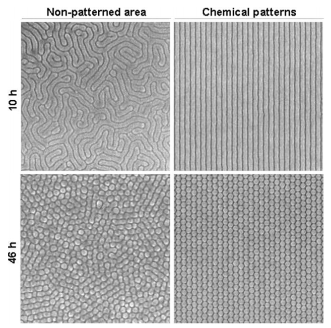
Fabrication of nanopatterns or nanostructures at a surface is often limited to the accuracy and resolution of the instrument. Photolithography is successful at producing nanostructures, but the properties are restricted to the dimensions of the chosen mask. In a current Soft Matter article, a collaborative research group has added an additional step to traditional photolithography to produce more complex micro- and nanostructures. Initially, nano ‘pre-patterns’ were formed on substrates with photolithography; cross-linked polystyrene (PS), poly(methyl methacrylate) (PMMA), or a hydroxyl terminated polymer (PS-PMMA-OH) were patterned as nanostripes on a silicon wafer surface. After the patterns were deposited, a second layer of block copolymer, PS-b-PMMA, was spincoated over the entire pre-pattern. Finally, samples were incubated in a sealed container with an open vial of acetone to anneal the layer of PS-b-PMMA. The solvent annealing of the block copolymer produced ordered nanostructures of PS-b-PMMA on top of the premade photolithography pattern. PS-b-PMMA structures and dimensions varied with annealing time but remained ordered due to the initial chemical pre-pattern. Unpatterned surfaces also developed nanostructure, but without any order to the polymer structures.
The mechanism of assembly of the block copolymer nanostructures was controlled by two factors: film thickness and migration of PMMA polymer chains from the bottom to the top of the surface as PMMA is more stable in an acetone vapor. The combination of solvent annealing and chemical pre-patterning perturbs the polymer chain configurational energy and interfacial energy to instigate the nanostructure formation. The polymer microdomains are formed while solvated and are retained after acetone removal. The control of nanopattern dimensions with chemical pre-patterning and solvent annealing expands the application range of traditional photolithography. This appealing fabrication procedure can be utilized by the seminconductor industry where complicated nanopatterns are used for data storage or electronics.
See the full Soft Matter article here:
Lei Wan, Shengxiang Ji, Chi-Chun Liu, Gordon S. W. Craig, and Paul F. Nealey
 Dr. Morgan M. Stanton is currently a postdoctoral researcher at the Max Planck Institute for Intelligent Systems in Stuttgart, Germany. She completed her Ph.D. in Chemistry from Worcester Polytechnic Institute in 2014. Read more about Morgan’s research publications here or you can follow her on Twitter @morg368.
Follow the latest Soft Matter publications and updates on Twitter @softmatter or on Facebook.


