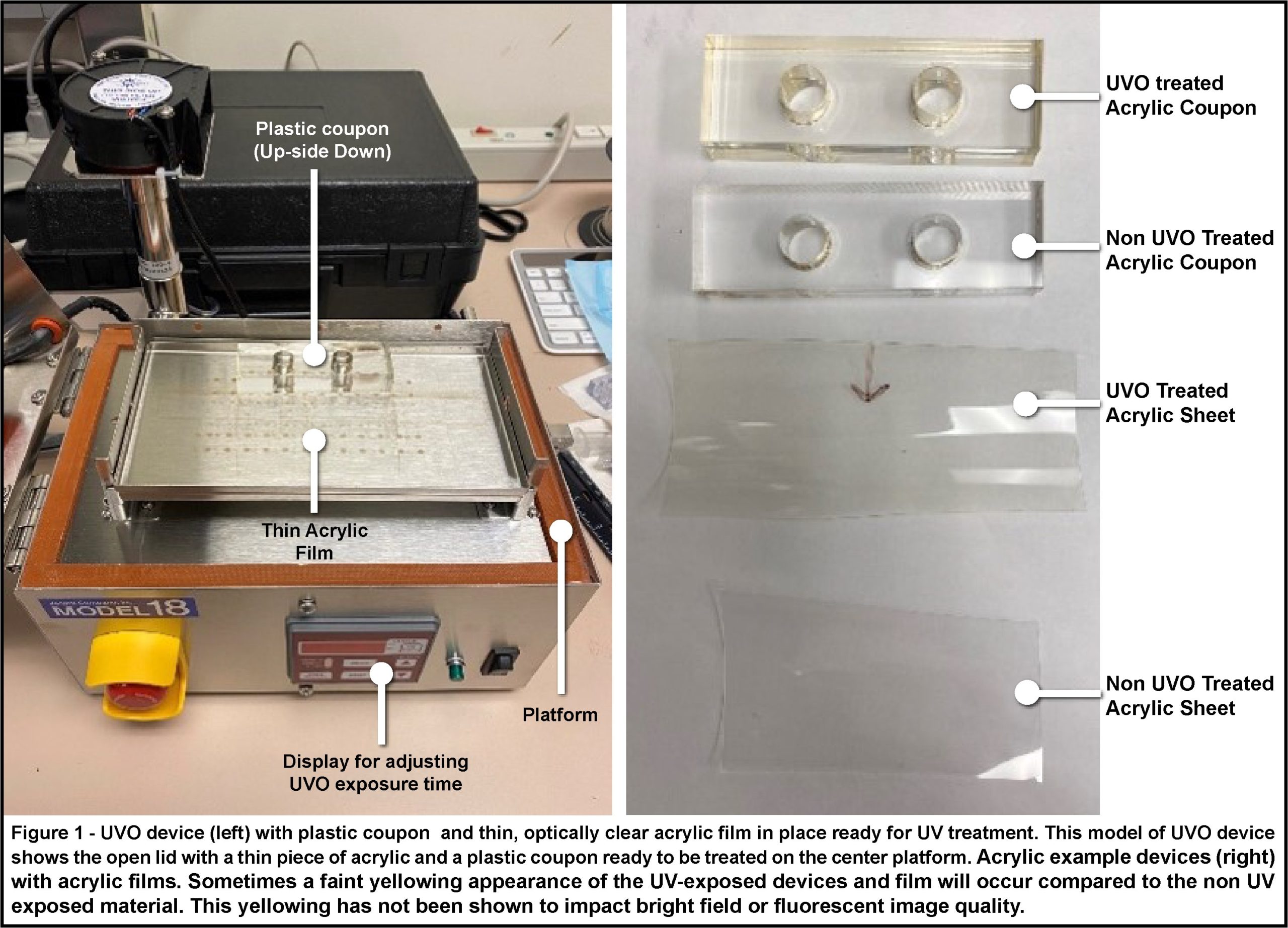
Sara E. Parker1 and Peter G. Shankles2, Maddie Evans1, Scott T. Retterer1,2,3
1 Biosciences Division, Oak Ridge National Laboratory, Oak Ridge, TN
2 The Bredesen Center, The University of Tennessee, Knoxville, TN
3 The Center for Nanophase Materials Sciences
Why is this useful?
Even simple microfluidic devices often require complex and expensive pumping and valving systems for accurately metering and controlling fluid flow. This often necessitates substantial and time-consuming set-up, and sometimes make these chips unwieldly and difficult to image. It can also represent a significant departure from the rather straight forward process of pipetting fluids from one small volume to another, making adoption by non-microfluidic experts unlikely. However, the development of well-plate microfluidics1,2 provides a high throughput, simplified method for studying fluid exchange and shear flow, while minimizing the set-up and need for multiple fluid connections. Creating an interface between the polystyrene (PS) plate and the polydimethylsiloxane (PDMS) fluidics presents the largest obstacle in creating these hybrid devices. Khine et al.1 utilized pressure to create a tight interface while Conant et al.2 adhered the surfaces using glue, but neither elaborated on their techniques and in practice small changes in the process can result in failed devices. Here, two techniques are detailed on consistently creating an effective interface between the well-plate and microfluidics. Resulting in individual wells that are interconnected via custom microchannels in a PDMS device attached to the bottom of the well-plate. Reagents are then added to wells and, driven through the underlying channel network into an outlet well via hydrostatic pressure or a pressure control system3,4.
With the use of this platform, flow can be introduced into traditional well-plate studies allowing various physiological conditions to be more closely mimicked. Further, the compatibility of these custom devices with well-plate microfluidic control systems provides the opportunity to precisely and dynamically control experimental conditions including temperature, pressure, and gas environment3,4. The use of multi-well plates also allows for multiple devices to be bonded in parallel to the same plate, increasing throughput without increasing the complexity of the control system5. Additionally, the familiarity and ubiquity of the well-plate platform provides a familiar platform for technical professionals within the lab and is automatically compatible with the host of microscope stage attachments already available for use with conventional well-plates.
Well-plate microfluidic fabrication has been shown with a pressure seal between the microfluidics and well-plate1 as well as gluing the two together2. This work builds off these ideas by detailing bonding with a liquid adhesive or chemical activation and bonding. The process of bonding customized PDMS devices to well-plates for well-plate microfluidics has only been vaguely described previously5,6. Herein, we present two approaches that utilize either (3-Aminopropyl)triethoxysilane (ATPES) to modify the surface of the PS well-plate to bond with plasma treated PDMS, or uncured PDMS to act as a glue between the PS and PDMS surfaces7. While the APTES modification provides a stronger bond without adding additional material, the uncured PDMS bonding procedure requires less pressure, avoiding any distortion of nanoscale features. An overview of the process is shown in Figure 1:
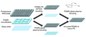
Figure 1 – Diagram of the fabrication process with the APTES process above and PDMS glue below.
What do I need?
Materials
- PDMS device replica with inlets and outlets designed to align with a well-plate
- 48 well-plate; Flat-bottomed, non-tissue culture treated
- Isopropyl alcohol (IPA)
- Coverslip or slide large enough to cover channels
- X-Acto knife
- Scotch tape
APTES bonding only
- APTES
- Deionized water
- Hard rubber brayer
- Sealable plastic container
PDMS bonding only
- Tapered tip plastic syringe (Nichiryo 6mL syringe with tips)
- Uncured PDMS (10:1 w/w elastomer base to curing agent)
Equipment
- Drill press
- Plasma cleaner (Harrick Plasma, Basic plasma cleaner PDC-32G)
- Hot plate
- Oven (75°C)
What do I do?
Well-plate preparation (for both bonding methods)
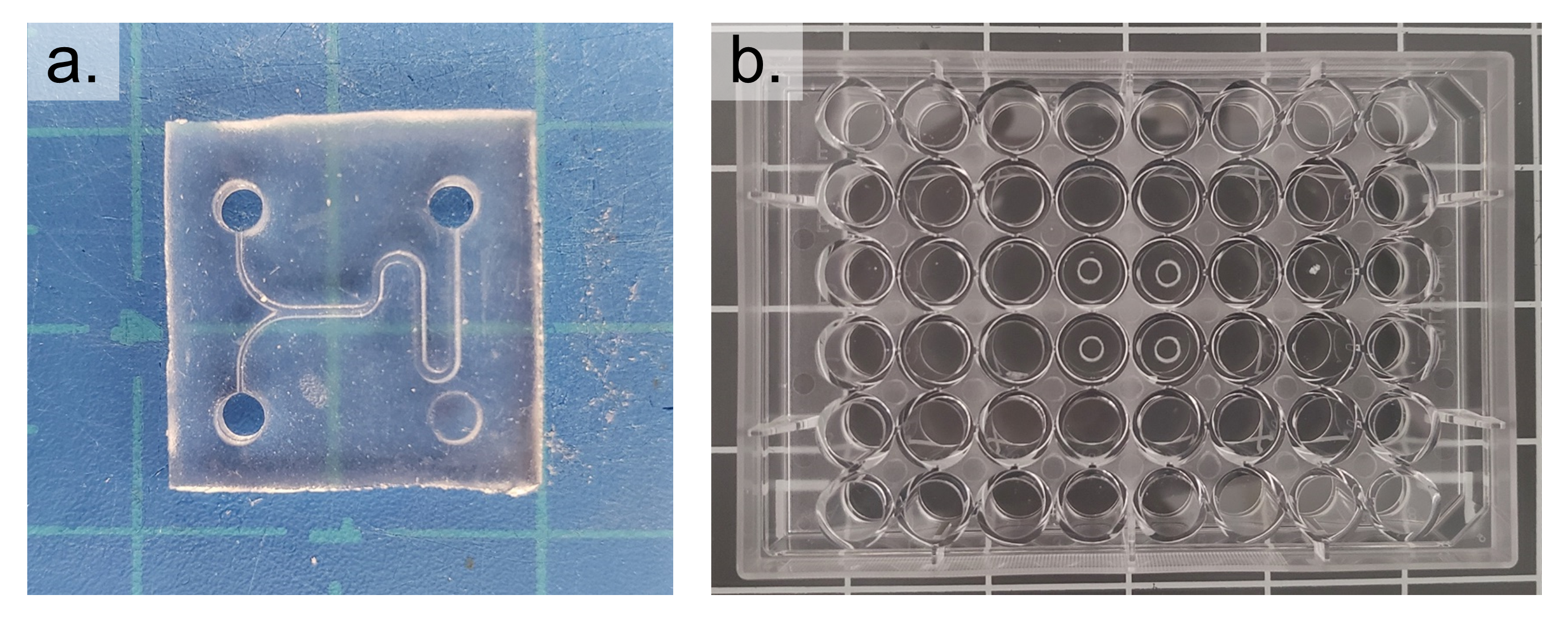
- Prepare the well-plate by drilling a hole in the center of each well corresponding to an inlet or outlet on the PDMS replica (Figure 2).
- Using an X-Acto knife, clean the edges of the drilled holes such that the bottom surface of the well-plate is smooth and any lips that may have formed from drilling have been removed.
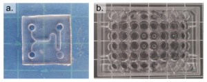
Figure 2 – The prepared PDMS device is shown in a. and the prepared well-plate is shown in b.
APTES bonding Procedure
Well-plate APTES modification
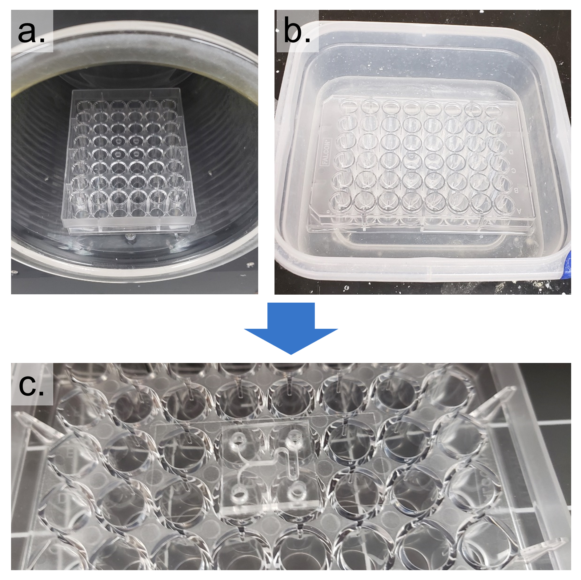
1. Clean the bottom surface of the well-plate with IPA and expose to oxygen plasma on high setting for 2 minutes, with the bottom surface of the plate facing up (Figure 3a).
2. In a fume hood, prepare a 100 mL aqueous solution of 1% v/v APTES and pour the solution into a shallow, resealable container.
3. Place the plasma treated well-plate in the APTES container so that the bottom surface of the plate is completely submerged. Seal the container and let soak for 30 minutes (Figure 3b)
4. Remove the plate from the APTES bath and rinse the top and bottom with water. Dry the well-plate using compressed air and place it on a 50°C hot plate to ensure thorough drying.
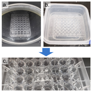
Figure 3 – The well-plate was exposed to air plasma and submerged in a water/APTES solution to modify the surface chemistry and enable bonding between PS and PDMS. A coverslip was then plasma bonded to the PDMS surface.
Assembly
1. Clean the top of the PDMS replica (opposite to the channels) using scotch tape and plasma clean on high for 1 minute.
2. With the channeled side of the PDMS replica facing up, align the inlets/outlets of the replica with the holes of the APTES-modified well-plate and press the layers together. Roll a brayer over the surfaces to remove any bubbles and ensure an even, uniform bond. Bake at 75°C for 20 minutes (Figure 3c).
3. Remove the well-plate with bonded device from the oven and use scotch tape to remove debris from the channel-exposed PDMS. Clean a glass coverslip with IPA and expose the coverslip and well-plate to oxygen plasma on high for 1 minute. Bond the coverslip to the PDMS replica, thus enclosing the channels and bake at 75°C for 20 minutes.
Uncured PDMS procedure
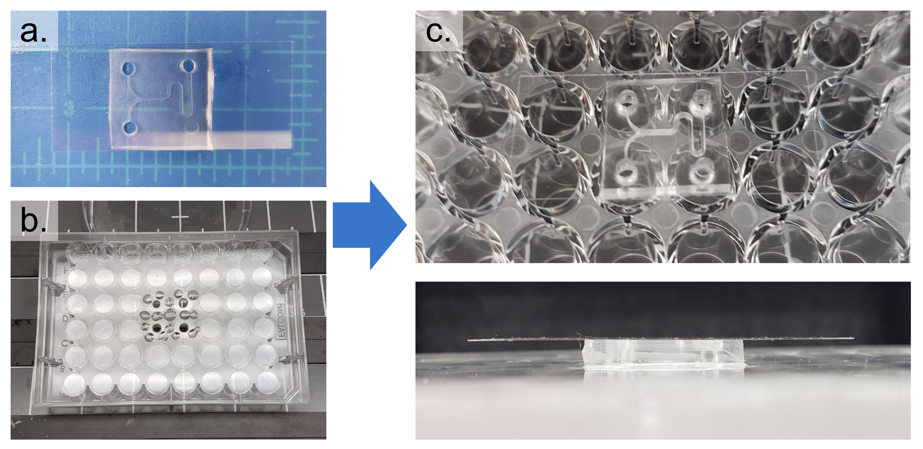
1. Remove any dust from the bottom (channel-exposed) side of the PDMS replica using Scotch tape and clean a glass coverslip with IPA. Expose both to oxygen plasma for 1 minute on high setting and bond them together, enclosing the channels. Bake at 75°C for 1 hour (Figure 4a).
2. Clean the bottom surface of the prepared well-plate with IPA. Using the tapered tip syringe, place small droplets of uncured PDMS onto the bottom surface of the well-plate where the PDMS device will be bonded (Figure 4b).
3. Using scotch tape, remove any dust from the top (opposite to the channels) of the coverslip-bonded PDMS replica. Align the inlets/outlets of the device with the holes of the well-plate and lightly press the device onto the well-plate (Figure 4c). Remove any uncured PDMS that may have leaked into the wells or inlets/outlets of the device. Bake at 75°C for 1 hour.
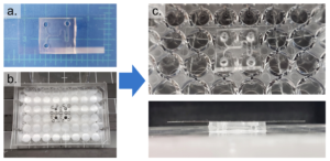
Figure 4 – The PDMS device was first bonded to a coverslip (a) and then bonded to a well-plate using uncured PDMS (b). c shows the completed device from the top and side view.
Conclusion
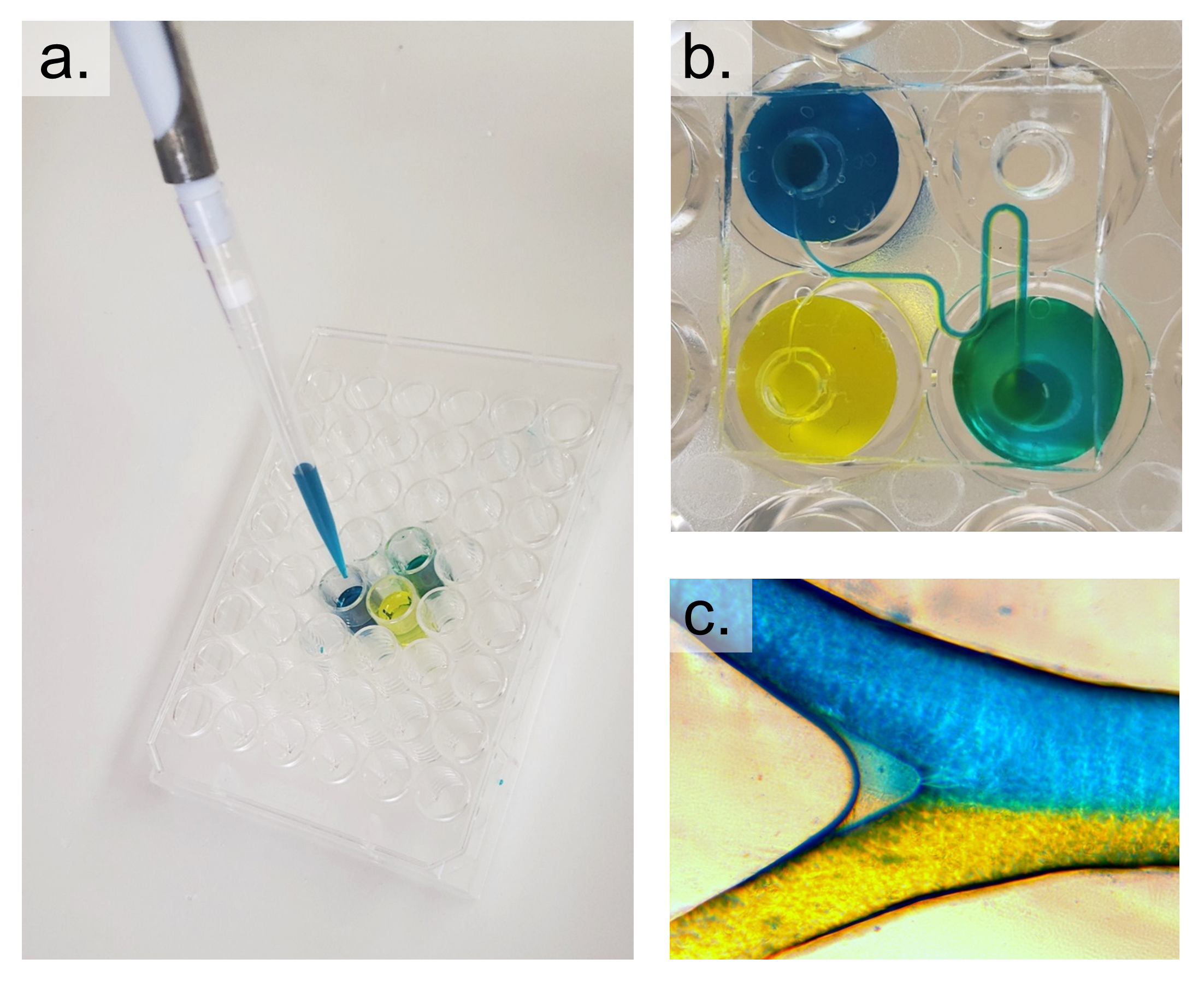
We present two methods for attaching PDMS microfluidic devices to polystyrene well-plates, providing the opportunity to utilize customized channels for well-plate microfluidics. Assays using these devices can be run in conjunction with well-plate microfluidic controllers or using simple pipetting methods by adding the desired reagent or media to the inlet wells (Figure 9). While the fabrication process is more involved than typical PDMS processing, well-plate microfluidics removes the need for complicated tubing connections by working with a single manifold controller, or hydrostatic flow using the well height to produce pressure.

References
1 M. Khine, C. Ionescu-Zanetti, A. Blatz, L. P. Wang and L. P. Lee, Lab Chip, , DOI:10.1039/b614356c.
2 C. G. Conant, M. A. Schwartz, J. E. Beecher, R. C. Rudoff, C. Ionescu-Zanetti and J. T. Nevill, Biotechnol. Bioeng., , DOI:10.1002/bit.23243.
3 Fluxion, White Pap., 2008, 1–6.
4 2012, US00825796.
5 C. G. Conant, J. T. Nevill, M. Schwartz and C. Ionescu-Zanetti, J. Lab. Autom., 2010, 15, 52–57.
6 P. J. Lee, N. Ghorashian, T. A. Gaige and P. J. Hung, J. Lab. Autom., , DOI:10.1016/j.jala.2007.07.001.
7 V. Sunkara, D.-K. Park, H. Hwang, R. Chantiwas, S. a. Soper and Y.-K. Cho, Lab Chip, 2011, 11, 962–965.
Comments Off on Cutting the cords: Two paths to well-plate microfluidics


")