Archive for the ‘Chips n Tips’ Category

Threadless chip-to-world connections on resin 3D printed microscale devices

Hannah B. Musgrove, Rebecca R. Pompano

Department of Chemistry, University of Virginia

Email: hbm8g@virginia.edu, rpompano@virginia.edu


Why is this useful?

With the continued adoption of 3D printed fabrication for microfluidics, the ability to easily connect non-elastomeric, resin 3D printed devices to fluidic tubing is an ongoing area of optimization. Common strategies to connect tubing to printed chips involve incorporating threading for use with luer lock adaptors, or embedding flanges or O-ring into devices.1–5 While useful for many types of inlets, standard luer adaptors are often > 10 mm in scale and thus too large for smaller chip designs. Additionally, the quality of 3D printed threading depends on the resolution of the printer and resin material, and the threads may wear down with repeated use. Embedding flanges1 or O-rings at connection sites6,7 may alleviate some of these print related limitations and increase the durability of the tubing ports. However, they also require additional manual fabrication steps including gluing or embedding parts and alignment. These extra steps are time-consuming and can increase fabrication inconsistencies. A simple option is to add a tubing-sized hole into a channel design which can be printed easily.6,7 This is similar in concept to dermal punching methods common for polydimethylsiloxane (PDMS)-based chips.1,4 However, while the soft, elastic properties of PDMS allows for a secure connection with tubing-sized holes, most 3D printed materials are more rigid, preventing conformal contact.

To address these issues, we developed a simple, threadless design for a raised port, that produces durable, 3D printed connection sites for tubing. We have used it successfully with both low and high viscosity vat-polymerization 3D printing resins (MiiCraft BV007a and FormLabs Clear, respectively) and compared it with, fused deposition fabrication of the same port using polylactic acid filament. This design is intended to decrease fabrication time and can be used with or without additional commercial adapter parts.

What do I need?

Basic materials are listed first, with the specific tools that we used listed in parenthesis.

  • Vat-polymerization 3D printer (MiiCraft P110Y, 385 nm 3D printer)
  • Resin (MiiCraft BV007a, or FormLabs BioMed Clear)
  • 3D design software (Fusion360 with Education License)
  • Microfluidic tubing, 1/16” OD or smaller (1/32” PTFE, 1/32” PEEK, and 1/16” silicon peristaltic tubing)
  • Optional: Ferrule lock rings (Idex Super Flangeless Ferrule, Cole-Parmer)

Measurement components for design

  • Included 3D software files or blueprint in Figure 1
  • Outer diameter (OD) of tubing being used
  • Estimate of print shrinkage and tolerance needed

What do I do?

  1. With 3D designing software, open the design to which you wish to add tubing connection ports.
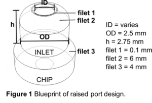
  2. Above each port location, create a cylinder 2.75 mm tall with a 2.5 mm outer diameter ( 1). These are the standard dimensions that will fit with the optional ferrule locks in later steps.
  3. A hole in the center of the cylinder should be created to reach from the top of the cylinder down to the channel or port of the chip (“ID”, 1). The diameter of this hole should be customized to best fit the outer diameter of the tubing being used. (See next section for tips.)
  4. Filets should be added at three key locations ( 1).
    1. Filet 1 is at the edge of the inner cylinder hole and is set to 0.1 mm.
    2. Filet 2 is at the top, outer edge of the cylinder and is set to 6 mm.
    3. Filet 3 is at the base of the cylinder where the port meets the chip and is set to 4 mm.
  5. Once the raised port designs are added to the chip, use your printing software to orient and build supports for the print as needed ( 2A)
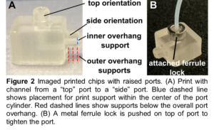
    1. Ports located on the “top” face of the chip (facing away from the baseplate during printing) do not require supports.
    2. Ports located on the “side” faces of the print do typically require at least one support for both the inner diameter and outer diameter overhangs
  6. Once printed and post-processed, tubing should fit directly into the ports, with close, conformal contact.
  7. Optionally, for further connection support, a ferrule lock can be used:
    1. Start by sliding the ferrule lock over the tubing before inserting the tubing into the raised port.
    2. Once inserted, slide the ferrule lock over the raised port ( 2B) to gently tighten the port around the tubing.

What else should I know?

The raised port designs were compared to a printed chip-to-syringe female thread luer inlet and a simple printed hole in the chip, and tested by driving flow through a simple microfluidic channel. We tested printability, ability to maintain a seal during multi-day fluid flow, and ability to be re-used without wearing down in two different resins (MiiCraft BV007a and FormLabs Clear). We also attempted to print the design using a fused deposition modeling (FDM) printer.

For printability, the raised port and simple hole designs printed successfully more often in resin printed chips than did luer lock ports, likely due to size and lack of threading.

For reuse, we found that the raised ports typically retained a good seal with the tubing through > 20 rounds of inserting, removing, and re-inserting tubing, in both FormLabs and MiiCraft resins. Use of the ferrule lock enabled additional re-use of resin printed raised ports. In comparison, simple embedded holes wore down ~7x reuse on average. This is likely due to faster wear around the edges from mechanical stress, from repeated use in addition to forces from material shrinkage that act on the hole by the surrounding printed shape.8

For durability of the connection, prolonged use of the ports was tested over one week by continually pumping saline solution through single-channel chips at 37°C at a rate of 1 µl min-1. It was found that the quality of the seal was primarily limited by resin stability under these conditions, rather than by mechanical wear at the port. Chips printed with BV007a resin began to leak and deform at both the port site and other channel locations after 48 hours, whereas chips with FormLabs Clear resin were stable for at least 5 to 7 days without any noticeable signs of leaking or wear at the ports. These results are consistent with our prior findings that BV007a prints are sensitive to extended heat treatment.8 We conclude that the port design is likely to yield a durable seal as long as the material is stable under the conditions of the experiment.

For additional stability, ferrule locks can also be added to further support and increase the duration of tubing-to-chip connections, especially for devices experiencing challenges with backpressure.

This design for ports works best with resin/vat-polymerization printers that have high print resolution (i.e. are able to print features around 1 mm in scale or lower) and with materials that are stiff yet slightly pliable, such as the listed resins. This design could in principle be adapted for high resolution fused deposition (FDM) printing but would again fair better with slightly pliable materials; we found that more rigid plastics such as polylactic acid (PLA) were difficult to combine with soft tubing, especially if FDM print tolerance is inconsistent.

Several design files are included for convenience on our dataverse website (https://dataverse.lib.virginia.edu/dataverse/PompanoLab). These files can be used “as is” to test fit with the tubing of interest or can be edited and added to an existing chip design.

Conclusion

The inlet design demonstrated in this work was found to be durable, versatile, and simple to fabricate for microfluidic chips printed with resin 3D printers. Though other systems work well for larger chips, the design shown here can be used when a smaller inlet connection is needed.

Acknowledgements

Research reported in this publication was supported by the National Institute of Allergy and Infectious Diseases under Award No. R01AI131723 and from the National Institute of Biomedical Imaging and Bioengineering under Award No. R03EB028043 through the National Institute of Health (NIH). The content is solely the responsibility of the authors and does not necessarily represent the official views of the National Institutes of Health.

References

  1. Price, A. J. N., Capel, A. J., Lee, R. J., Pradel, P. & Christie, S. D. R. An open source toolkit for 3D printed fluidics. J. Flow Chem. 11, 37–51 (2021).
  2. van den Driesche, S., Lucklum, F., Bunge, F. & Vellekoop, M. 3D Printing Solutions for Microfluidic Chip-To-World Connections. Micromachines 9, 71 (2018).
  3. Au, A. K., Huynh, W., Horowitz, L. F. & Folch, A. 3D-Printed Microfluidics. Angew. Chem. Int. Ed. 55, 3862–3881 (2016).
  4. Anderson, K. B., Lockwood, S. Y., Martin, R. S. & Spence, D. M. A 3D Printed Fluidic Device that Enables Integrated Features. Anal. Chem. 85, 5622–5626 (2013).
  5. Weisgrab, G., Ovsianikov, A. & Costa, P. F. Functional 3D Printing for Microfluidic Chips. Adv. Mater. Technol. 4, 1900275 (2019).
  6. Bhargava, K. C., Thompson, B. & Malmstadt, N. Discrete elements for 3D microfluidics. Proc. Natl. Acad. Sci. 111, 15013–15018 (2014).
  7. Ji, Q. et al. A Modular Microfluidic Device via Multimaterial 3D Printing for Emulsion Generation. Sci. Rep. 8, 4791 (2018).
  8. Musgrove, Hannah. B., Catterton, Megan. A. & Pompano, Rebecca. R. Applied tutorial for the design and fabrication of biomicrofluidic devices by resin 3D printing. Anal. Chim. Acta 1209, 339842 (2022).
Digg This
Reddit This
Stumble Now!
Share on Facebook
Bookmark this on Delicious
Share on LinkedIn
Bookmark this on Technorati
Post on Twitter
Google Buzz (aka. Google Reader)

VGA-inspired tubing connectors to operate microfluidic chips

Imre Banlaki, Horst Henseling, Henrike Niederholtmeyer

Max Planck Institute for Terrestrial Microbiology, Marburg

Why is this useful?

As microfluidic chips increase in complexity, more and more tubes need to be connected to a chip for operation. That is especially the case where many pneumatic valves (“Quake valves”) are included in the design of two-layer devices [1,2]. In many cases, these valves are actuated by a central, electronic switch board, driving solenoid valves [3]. The central switchboard makes each individual valve easily programmable for multiple applications.

The drawback of this versatile set up is the need to rewire all connectors to a new chip to initiate the experiment. This is time consuming and increases the likelihood of human error, especially if the setup is used by multiple researchers, who use different chips.

A plug and play solution would allow each researcher to have their personal end pieces connected to their chips and interfacing with the switchboard. This allows preparation on the lab bench and facilitates the change from one experiment to another.

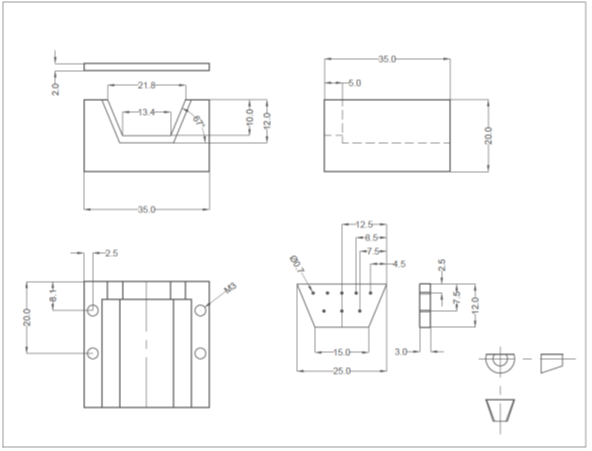
To that end, we designed a 3D printable mould to cast PDMS trapezoids with 8 integrated tubes (Fig. 1). The shape and tube-pattern make the connector unambiguous, similar to a VGA or D-sub electronics connector. A D-sub microfluidic connector of similar design has been published before, however it relies on actual, disassembled D-sub connectors which have gone out of fashion [4].

What do I need?

PDMS Sylgard, Dow Corning
Resin 3D printer or other means of fabrication
Tygon tubing (0.51 x 1.52 mm) or other as preferred
Blunt dispensing needles 23G (0.43 x 0.64 mm)
Scissors
Pliers
Glass petri dish
4x M3x20 screws and nuts

Figure 1 Blueprint of the pieces to fabricate and assemble the mould. Measurements in mm.

How do I do it?

  1. Fabricate the mould

3D print or mill the mould from a thermally stable resin, polymer or noncorrosive metal. We have shared our design on Metafluidics.org. (https://metafluidics.org/devices/vga-inspired-tubing-connector/)

Drill the holes in the trapezoid plate. Make sure the hole-array is axisymmetric by measuring each placement from the middle.

  1. Prepare the mould

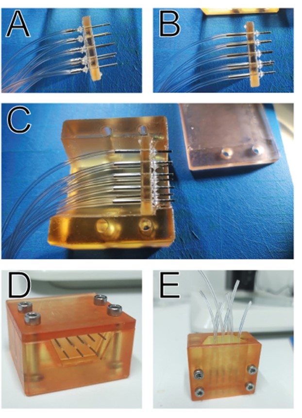
Remove 8 metal pins from the plastic of the blunt dispensing needle tips. Cut 8 approx. 3-5cm Tygon tubing pieces and push them onto the end of the metal pins that was inserted in the plastic.

Insert the pins + tubing into the holes of the trapezoid plate (Fig. 2A).

Place the plate into the notch of the mould with the pins sticking out towards the shorter end, and screw the top plate on (Fig. 2C+D).

Figure 2 Assembly steps of the mould. A) Pins and tubing inserted in the trapezoid plate to fabricate a plug. B) Pins and tubing inserted in the plate to fabricate a socket. C) Plate, with pins and tubing, placed into the grove before adding the top plate. D) Fully assembled mould with flush pins sticking out. E) Vertical placement of assembled mould ready to be filled.

  1. Cast the PDMS

Mix 10g PDMS resin (1:10 as per supplier instruction).

Place the mould vertically so the hole is on top (Fig. 2E). Make sure the pins are flush with the bottom (use the petri dish). Arrange the bend of the tubing in a way that makes it easy to identify which tube belongs to which pin.

Cast the PDMS until at least 50% of the mould is filled.

Cure in the oven at 80°C for 30-60 mins.

  1. Remove the connector

After curing, unscrew and remove the top plate. Carefully remove the PDMS piece including the trapezoid plate from the mould. Now, you should be able to slide the plate off the pins.

The tubing on the back end is now ready to be connected to tubing from a control board by individual bridging with metal pins. The front end forms the quick connector for 8 lines.

  1. Setup for receiver socket

To cast a receiver socket, insert 8 metal pins without tubing into the trapezoid plate. Now connect some tubing to the pins so that the plate is sandwiched between pin and tubing (Fig. 2B). Insert the assembly into the mould as before and cast the PDMS. After curing and removal of the piece, the metal pins can be pulled out leaving only the tubing embedded within the PDMS.

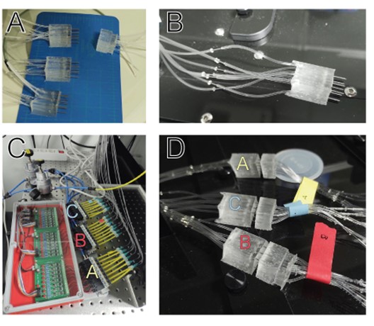
Figure 3 Plugs and socket A) after removal from the mould and B) connected to the switch board. C) Switch board with 24 valves clustered into 3×8 (A, B, C) control lines. D) Three plugs (A, B, C) connected to sockets.

What else should I know?

Curing without degassing may create bubbles, and depending on the resin for 3D printing the surface may remain somewhat sticky. This will not affect functionality. The stickiness can be avoided by placing the mould in isopropanol for a few days. Adding pigment to the PDMS could be used to colour code each plug. Expanding the design for more lines should be possible but connecting will be increasingly difficult.

Uncareful connection, puncturing the PDMS, may clog a pin.

When milling the device, instead of 3D printing, it is advised to change the plate shape and notch to a semi-circle and mill on the face to guarantee a flush fit of the plate.

Acknowledgements

This work was supported by Deutsche Forschungsgemeinschaft grant NI 2040/1-1.

References

  1. Unger MA, Chou H-P, Thorsen T, Scherer A, Quake SR. Monolithic Microfabricated Valves and Pumps by Multilayer Soft Lithography. Science. 2000;288: 113–116. doi:10.1126/science.288.5463.113
  2. Niederholtmeyer H, Stepanova V, Maerkl SJ. Implementation of cell-free biological networks at steady state. Proc Natl Acad Sci. 2013;110: 15985–15990. doi:10.1073/pnas.1311166110
  3. Brower K, Puccinelli RR, Markin CJ, Shimko TC, Longwell SA, Cruz B, et al. An open-source, programmable pneumatic setup for operation and automated control of single- and multi-layer microfluidic devices. HardwareX. 2018;3: 117–134. doi:10.1016/j.ohx.2017.10.001
  4. Scott A, Au AK, Vinckenbosch E, Folch A. A microfluidic D-subminiature connector. Lab Chip. 2013;13: 2036–2039. doi:10.1039/C3LC50201E
Digg This
Reddit This
Stumble Now!
Share on Facebook
Bookmark this on Delicious
Share on LinkedIn
Bookmark this on Technorati
Post on Twitter
Google Buzz (aka. Google Reader)

A simple, efficient, and cost-effective spin coater: A waste to wealth approach

S.J.Samuel Justin1, P.Wilson1

1Department of Chemistry, Madras Christian College

Email: sam310just@gmail.com, wilson@mcc.edu.in


Why is this useful?

Spin-coating is a highly reproducible, simple, time-efficient, and cost-effective coating technique is widely employed technique for the fabrication of thin-film coatings over large areas with smooth and homogeneous surfaces [1]. It has been widely used for the production of monolayer- and multilayer-thin coatings, freestanding (FS) nanosheets and membranes, for various industrial and biomedical applications, e.g. mitigation of corrosion [2], wound dressings, cell culture substrates, and as drug delivery devices.

A tip to develop portable spin coaters by recycling computer fans and mobile phone wall chargers was previously presented [3]. Using adhesive strips to secure a metal alloy sample on the center of the computer fan often slips and knocked down while trying to remove the sample after the coating process. This affects the coating and thereby a proper substitute to hold the sample tight during the spin and at the same time easier to remove it after the coating is essential. In addition, the sample spinning at high rpm levels expels the excess coating substrate away from the system which has to be addressed in order to prevent the contamination of the surroundings. In this regard an improved form of portable spin coater is proposed and presented.


What do I need?

Parts for the spin coater

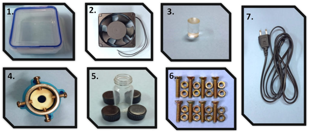
  1. Polycarbonate container, Dimensions 155 X 155 X 60 mm
  2. Panel cooling fan 120 x 120 x 38 mm with 2800 rpm
  3. Acrylic support rod of length 15 mm and diameter of 12 mm
  4. Faucet water tap adapter
  5. Black cap of 5mL clear round glass bottle – 4 pieces
  6. 8 pieces set of 3mm diameter round head 20 mm bolt and nut
  7. Power cable

Parts and chemicals for the specific examples

  • Nitro cellulose lacquer
  • Aluminium alloy 15mm x15mm x6mm


What do I do?

Assembling of spin coater

  1. The acrylic rod is fixed at the centre of the fan using instant cyanoacrylate ester adhesive (Fig.a)


  1. A hole of 15 mm dia. is drilled at the centre of the container base and 2.8 mm hole at the four corners of the container (Fig.b).
  2. The container is placed over the fan and the corners are fixed using bolt and nut (Fig.c)
  3. The stem of the faucet water tap adapter was cut and the hole is enlarged to 12mm dia. It is then fixed using instant adhesive on the top of the acrylic rod (Fig.d, e & f)

  1. The black caps were drilled at the center to create a hole of 2.8mm dia. The bolt is inserted from below each cap and then tightened with the base of the cooling fan at the four corners (Fig. g and h).
  2. The power cable is attached to the fan (Fig. i)

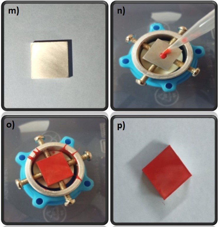
  1. The lid of the container is drilled at the center to 15mm dia. which acts as a space for dropping the coating material (Fig. j and k) and the final product is displayed in (Fig. l).
  2. The liquid containing the coating material (pigmented nitrocellulose lacquer) is placed on top of                 the substrate (Aluminium alloy) (Fig. m) by using a (micro) pipette (Fig. n.)
  3. The fan is turned on and the substrate is spin coated for about 30 seconds (Fig. o) (time can vary    depending on the substrate viscosity and coating thickness required). The coated substrate (Fig. p) is subjected to further evaluation.


References:


[1] Moreira, Joana, A. Catarina Vale, and Natália M. Alves. “Spin-coated freestanding films for biomedical applications.” Journal of materials chemistry B 9, no. 18 (2021): 3778-3799.

[2] Telmenbayar, Lkhagvaa, Adam Gopal Ramu, Daejeong Yang, Minjung Song, Tumur-Ochir Erdenebat, and Dongjin Choi. “Corrosion resistance of the anodization/glycidoxypropyltrimethoxysilane composite coating on 6061 aluminum alloy.” Surface and Coatings Technology 403 (2020): 126433.

[3] A second life for old electronic parts: a spin coater for microfluidic applications, https://blogs.rsc.org/chipsandtips/2018/04/25/a-second-life-for-old-electronic-parts-a-spin-coater-for-microfluidic-applications/ (accessed August 2020)

Digg This
Reddit This
Stumble Now!
Share on Facebook
Bookmark this on Delicious
Share on LinkedIn
Bookmark this on Technorati
Post on Twitter
Google Buzz (aka. Google Reader)

The Name is Bond – Heat Bond: Using a Heated Lamination Press for Thermoplastic Thin Film Bonding

Travis Swaggard1, Johanna Bobrow1, Peter Carr, Isabel Smokelin1, Todd Thorsen1, Christina Zook1, David Walsh1

1MIT-Lincoln Laboratory, 242 Wood St, Lexington, MA 02421


Why is this useful?

Have you ever tried to bond a thin clear bottom to your custom thermoplastic microfluidic device for high magnification microscopy? The bonding process can be cumbersome and relies on the heating temperature, the pressure placed on the device assembly, surface chemistry, as well as many other factors.1 We have developed a method that utilizes a heated laminator press and a UVO oven, which together cost less than hiring an external vendor who will likely charge per design and item manufactured. Currently, manufacturing bonded devices in-house can be difficult, expensive, and time consuming.

The new paradigm in microfluidic device prototyping using high-resolution 3D-printing has significantly reduced the barrier to participate in microfluidics, which traditionally required dedicated infrastructure and specialized expertise.2 However, once the design-build-test prototyping cycle has gone beyond the 3D-printing stage, additional prototyping in thermoplastics (e.g. CNC milling) is typically required for eventual scale-up using traditional hot embossing or injection molding manufacturing techniques. One of the critical challenges at this stage is placing optically-clear bottoms below the thermoplastic microfluidic device for optical interrogation, while withstanding fluidic flow and pressure. For example, adhesive bonding such as using double-sided tape can be tricky and tedious to align, and solvent-based adhesives can be messy or challenging to avoid impacting thin-film clarity, and even pose environmental safety concerns.

We have developed an inexpensive bonding protocol which can utilize almost any commercially available heated machine press to mitigate the aforementioned drawbacks, and bond layers of thin (125 micrometer) acrylic film to any flat acrylic microfluidic device surface. This allows for a strong bond that can provide a clear bottom for high-resolution optical interrogation, such as using a confocal microscope, for example. New low-cost commercial UVO ovens (Jelight Model 18 – $3,000) and heated laminated presses (Nugsmasher $500 [Mini] – $7,000 [Pro Touch]) have helped enable democratization of the thermoplastic film bonding process.

Here is a detailed walkthrough for the preparation and assembly of these devices. We have included photos and figures from each step for reference and convenience.

What do I need?

  • Thin, optically clear acrylic film (e.g. Röhm GmbH Acrylite Film 99524 or similar)
  • Microfluidic device from cast acrylic (e.g. Protolabs – CNC Machined)
  • Scissors
  • Oven mitts (or equivalent)
  • Multipurpose Neoprene rubber sheet 6”x 6” x 1/16” (or equivalent heat-safe separator)
  • Heated lamination press (Premiere Manufacturing SKU: 714343996295 or similar)
    • Must apply pressures between 30 and 50 PSI (roughly finger-tight, part won’t move if pushed by a finger)
    • Must be able to heat up to 118 °C

How do I do it?

  1. Using scissors, cut piece(s) of thin, optically clear acrylic film slightly larger than your acrylic device (this will eliminate any alignment steps, you can cut the remaining excess after the device has been pressed). Your film should be about half an inch oversized on all edges of the device to ensure that it is completely covered
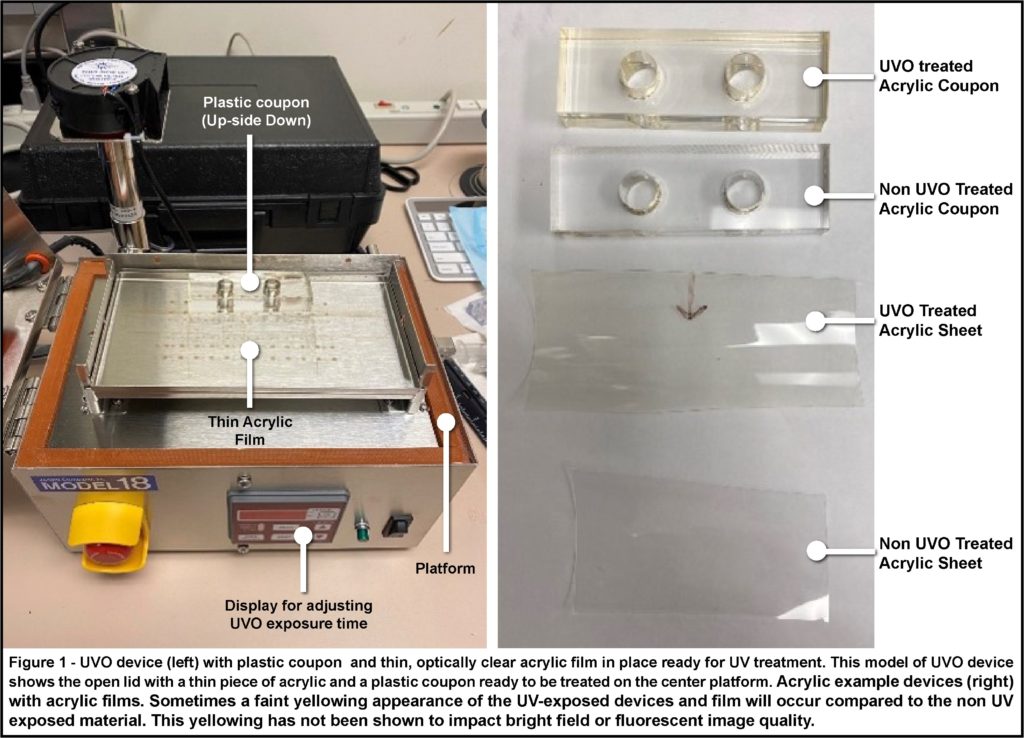
  2. Place the cutout of acrylic film(s) and plastic device(s) into the UVO oven so they are not touching and run for eighty minutes (see Fig.1). You can also perform oxygen plasma bonding alternatively; however, as that bond weakens over time, it’s important to perform the bonding immediately before the treatment. (Note: Be sure to put the bonding surfaces face-up in the UVO machine for best results.)
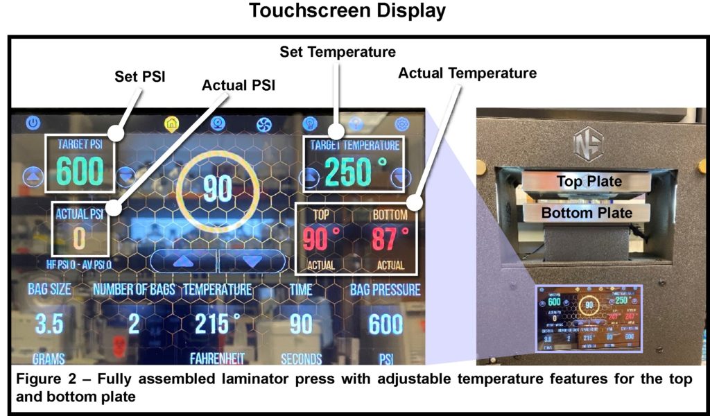
  3. Preheat laminated press to 118 °C (or about 250 °F). It may take up to twenty minutes to get up to temperature and an hour total to stabilize at the set point (see Fig.2).
  4. Very carefully (press will be very hot) place thin film on bottom plate and plastic device on top of film (use oven mitts or tongs for safety).
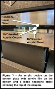
  5. Place a neoprene cover sheet over plastic coupon/film assembly. This will provide cushioning between the top press and your device and prevent any possible cracking or pitting from the top press (see Fig.3).
  6. Using the lever crank in the back, apply manual pressure until the machine registers a reading of 30-50 PSI (or roughly finger-tight, so the part won’t move if pushed by a finger or tong).
  7. Let device sit at steady pressure and heat, hold for ten minutes.
  8. Turn off heat but keep the device under pressure.
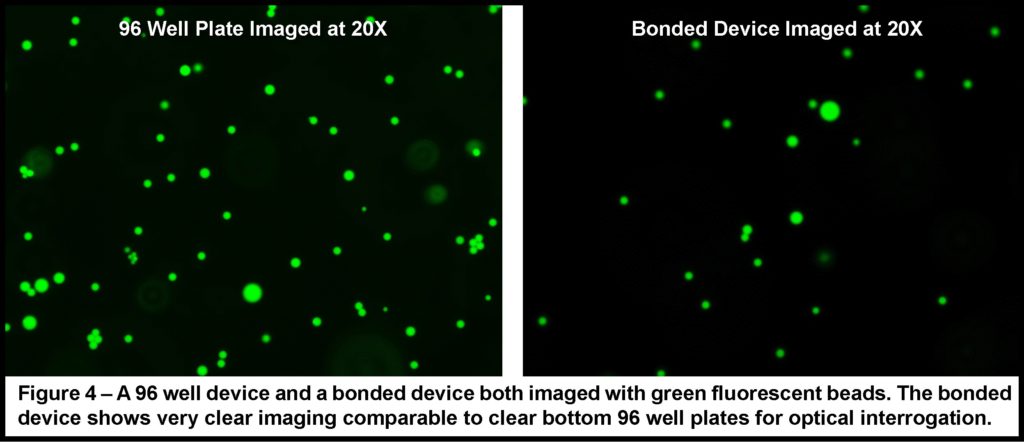
  9. Once heat returns to near room temperature, release pressure and remove device (Note: This may be overnight). Once complete, the devices should be effectively bonded and show optically clear bottoms with no aberrations (see Fig.4).

What Else Should I Know?

Before running this protocol, check your heated laminator press for scratches or pitting that could imprint on your film. If there are any significant scratches, these might become imprinted on your film and cause uneven bonding later in the process. A steel stainless steel sheet with a polished finish can be added on top of the bottom plate using thermal paste.

UVO treatment of plastics will create an oxide layer on the surface, rendering it more hydrophilic. The generation of oxygen species on the surface of plastics will reach a plateau after about sixty minutes.3

Almost any thermoplastic material4 can be bonded to the same type of material using the rule-of-thumb of heat being 5 °C over glass temperature, however it is worth noting that identical materials will bond most effectively, for example cyclic olefin polymer (COC) bonds to COC material straightforwardly, whereas COC will not bond as well to dislike material such as polycarbonate.

Do not overexpose your film and device to UVO (>sixty min) as this may cause significant yellowing and irreversible changes to the chemical makeup of the acrylic. Apply UVO as directed in this protocol. Some yellowing may happen, but in our hands, this does not create any noticeable background shading or autofluorescence.

Make sure not to put too much pressure on the film and device during the bonding process to ensure that devices are not warped, deformed or cracked, use only the pressure recommended in this protocol.

Always allow the heat from the laminated press to return back to room temperature, do not try to remove the device from the press before returning to room temperature as this will potentially produce an incomplete bonding.

If the pressure required for this bond causes deformation of critical features, consider applying ethanol to reduce surface glass temperature for a lighter pressure bond.5


While this publication discusses bonding to CNC-milled devices, there is potential for devices made from alternative fabrication techniques such as xurography or laser cutting to be bonded using a modified version of this protocol as well.6


Acknowledgements

We would like to acknowledge Chris Phaneuf, Ph.D. from Sandia National Laboratories as well as Edge Embossing (Charlestown, MA) for their assistance and expertise with helping us create this protocol. This work was funded by NIH/NCATS through an Interagency Agreement with MIT-Lincoln Laboratory as well as by NIH/NIBIB via grant award number 1R01EB025256-01A1.

© 2022 Massachusetts Institute of Technology.
Delivered to the U.S. Government with Unlimited Rights, as defined in DFARS Part 252.227-7013 or 7014 (Feb 2014). Notwithstanding any copyright notice, U.S. Government rights in this work are defined by DFARS 252.227-7013 or DFARS 252.227-7014 as detailed above. Use of this work other than as specifically authorized by the U.S. Government may violate any copyrights that exist in this work.


References

  1. Putting the Lid on Microfluidics [Internet]. Microfluidics. 2017 [cited 2022 Jan 7]. Available from: https://microfluidics.technicolor.com/wp-content/uploads/2021/12/Microfluidic-Chip-Bonding-Considerations-and-Case-Studies.pdf
  2. Bhattacharjee N, Urrios A, Kang S, Folch A. The upcoming 3D-printing revolution in microfluidics. Lab on a Chip. 2016;16(10):1720-42.
  3. Lin TY, Pfeiffer TT, Lillehoj PB. Stability of UV/ozone-treated thermoplastics under different storage conditions for microfluidic analytical devices. RSC advances. 2017;7(59):37374-9.
  4. Jiang J, Zhan J, Yue W, Yang M, Yi C, Li CW. A single low-cost microfabrication approach for polymethylmethacrylate, polystyrene, polycarbonate and polysulfone based microdevices. RSC Advances. 2015;5(45):36036-43.
  5. Harriet Riley, Development Editor. (2017, November 1). A solvent-based method to fabricate PMMA microfluidic devices – Chips and Tips. https://blogs.rsc.org/chipsandtips/2017/11/01/a-solvent-based-method-to-fabricate-pmma-microfluidic-devises/?doing_wp_cron=1625578271.8969628810882568359375 (Accessed November 2021)
  6. Burgoyne, F. (2010, May 17). Fast-iteration prototyping and bonding of complex plastic microfluidic devices – Chips and Tips. https://blogs.rsc.org/chipsandtips/2010/05/17/fast-iteration-prototyping-and-bonding-of-complex-plastic-microfluidic-devices/?doing_wp_cron=1625578517.8055989742279052734375 (Accessed November 2021)
Digg This
Reddit This
Stumble Now!
Share on Facebook
Bookmark this on Delicious
Share on LinkedIn
Bookmark this on Technorati
Post on Twitter
Google Buzz (aka. Google Reader)

INTERFACING MICROFLUIDIC CHIPS: DUAL CONNECTOR-RESERVOIR FIXTURE

Daniel Alcaide Martín, Jean Cacheux, Sergio Dávila & Isabel Rodríguez

Madrid Institute for Advanced Studies in Nanoscience (IMDEA Nanoscience), Ciudad Universitaria de Cantoblanco, C/Faraday 9, Madrid 28049, Spain

1- Why is this useful?

Microfluidic devices need to be connected to fluidic pumps for regulation of the flow during the device operation1. Connecting and disconnecting devices is a tedious and time-consuming operation that often causes air bubbles which are detrimental for the fluidic experiment and a real nuisance for the time it takes to eliminate them.

Furthermore, in microfluidic experiments dealing with biomolecules or cell cultures, volumes are of concern as these materials are typically limited and/or costly. Hence, it will be very useful if the reagent filling or replacement process and the connecting and disconnecting operations to microchips are minimized to avoid both bubbles and reagents waste. Reducing the reservoir volume to the volumes needed for the experiment minimizing dead volumes will also allow saving expensive reagents.

With this aim, we have designed a fixture to make practical fluidic connections to a microchip from a pressure controller for fluidic control and device operations. It allows for easy opening and closing operations and for easy re-filling or replacement of the reagents into the microchannels without moving any tubing connection.

Here, we present a dual connector cum reservoir fixture as a practical and effective means to making fluidic connections onto polydimethylsiloxane (PDMS) microfluidic based chips. The fixture is completely built by stereolithography (SLA) 3D printing and includes two components: a piece including a reservoir with an O-ring slit and a cone shaped outlet as chip connector and, another piece that closes the reservoir and has a cone shaped inlet or air pressure connector.

This Chips and Tips builds on a previous approach,2 dealing with microchip fluidic fixtures using magnets. However, in this case, the reservoirs and release connection are moved off the chip which would be more practical to work with the chip on the microscope stage for real time observations. Moreover, it is adaptable for any chip design and particularly for microchips made in soft PDMS.


2- What do I need?

  • 3D design software.
  • SLA 3D printer.
  • Cubic magnets.
  • O-rings.


3 – What do I do?

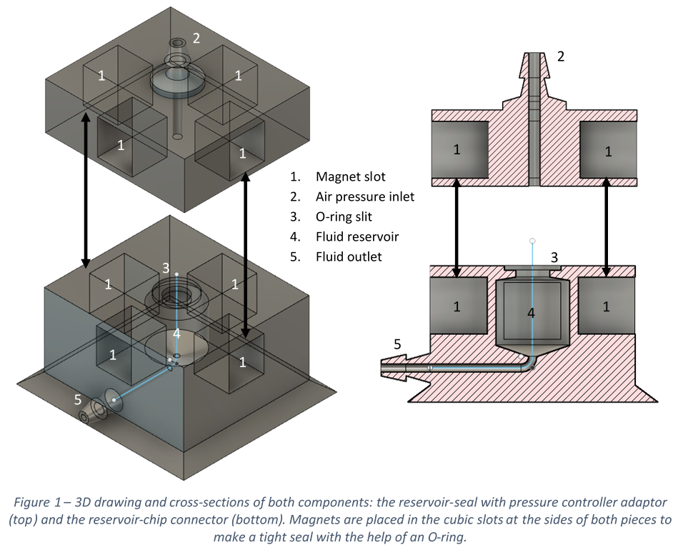
We first digitally design the parts of the dual connector: the reservoir-chip connector and the reservoir-seal air pressure adaptor. See the drawing in Figure 1. The corresponding F3D files can be here downloaded.

In our design, the reservoir sits aside from the PDMS chip and it is connected to it through a standard tube fitted on to the connecting outlet. The reservoir-seal encloses the reservoir. Four permanent magnets are inserted in each of the two components to produce a magnetic compressive force onto the O-ring and a tight seal to allow for applying a controlled pressure to cause the reagent to flow at the desired rate into the microfluidic chip.

Once the components are printed, the magnets are inserted into the lateral slots. Then, the plastic tubes are connected to the chip inlets and outlets and to the reservoir chip connector. The reservoir is filled with the correct volume of reagent (in this design is 0.2 ml) and the reservoir- seal piece is placed on top. Finally, through the air pressure inlet, tubing is connected to a pressure controller. When air pressure is applied, the reagent flows through the chip. The closing system formed by the O-ring seal and magnet force is able to handle at least 1 bar working pressure without any leakage.

Figure 2 – Fluidic system set-up showing .two dual connector-reservoir fixtures connected to a microchip and to a pressure controller.

Acknowledgements

This work was performed within the framework of the EVONANO project funded by the European Union’s Horizon 2020 FET Open programme under grant agreement No. 800983.

References

  1. Interfacing of microfluidic devices – Chips and Tips. https://blogs.rsc.org/chipsandtips/2009/02/27/interfacing-of-microfluidic-devices/.
  2. Reusable magnetic connector for easy microchip interconnects – Chips and Tips. https://blogs.rsc.org/chipsandtips/2011/06/27/reusable-magnetic-connector-for-easy-microchip-interconnects/.


Digg This
Reddit This
Stumble Now!
Share on Facebook
Bookmark this on Delicious
Share on LinkedIn
Bookmark this on Technorati
Post on Twitter
Google Buzz (aka. Google Reader)