A SERS biosensor for detecting metal ions in saliva

Written by Dr Lee Barrett.

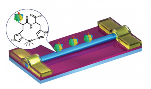
A gold nanohole array based surface-enhanced Raman scattering biosensor for detection of silver(I) and mercury(II) in human saliva

Researchers from West Virginia University have developed a method for detecting heavy metal ions in human saliva. Silver (I) (Ag) and mercury (II) (Hg) ions form part of dental fillings so it is important to have non-invasive analytical methods to monitor the toxicity of these metal ions should they be accidentally released into saliva.

Here, the authors exploited the strong electromagnetic coupling between gold (Au) nanostars and a Au nanohole array to detect Ag (I) and Hg (II) using surface enhanced Raman scattering (SERS). The Au nanostars and nanohole array were functionalised with mismatched pairs of single-stranded (ssDNA) probes that hybridise to form stable duplexes in the presence of the corresponding metal ions. Hybridisation allows the Au nanostars to come into close proximity with the Au nanohole array, which results in a large amplification of the SERS signal.

In this way, the authors were able to detect Ag (I) and Hg (II) ions in human saliva with limits of detection (LODs) of 0.17 nM and 2.3 pM for Ag (I) and Hg (II), respectively. This demonstrates the applicability of the SERS-based detection platform for on-site, non-invasive detection of analytes in body fluids.

A gold nanohole array based surface-enhanced Raman scattering biosensor for detection of silver(I) and mercury(II) in human saliva
Peng Zheng, Ming Li, Richard Jurevic, Scott K. Cushing, Yuxin Liu and Nianqiang Wu
Nanoscale, 2015, 7, 11005-11012. DOI: 10.1039/C5NR02142A

Dr Lee Barrett is a guest web writer for the Nanoscale blog. Lee is currently a postdoctoral researcher in the Centre for Molecular Nanometrology at the University of Strathclyde. His research is currently focused on the development of nanoparticle-based sensors and surface enhanced Raman scattering (SERS). Follow him on twitter @L_Bargie.

Digg This
Reddit This
Stumble Now!
Share on Facebook
Bookmark this on Delicious
Share on LinkedIn
Bookmark this on Technorati
Post on Twitter
Google Buzz (aka. Google Reader)

Poster prize winners at the 10th Sino-US Symposium on Nanoscale Science and Technology

Many congratulations to Chuanbo Gao and Mengyu Yan for winning the Nanoscale and Nanoscale Horizons poster prizes at the 10th Sino-US Symposium on Nanoscale Science and Technology.

Chuanbo, from the Xi’An Jiaotong University, and Mengyu, from Wuhan University, won prizes for their posters entitled “Etching-free epitaxial growth of gold on silver nanostructures for high chemical stability and plasmonic activity” and “Vanadium oxide/graphene nanocomposite for advanced lithium battery”, respectively.

The 10th Sino-US Symposium on Nanoscale Science and Technology took place from 26th to 28th June 2015 at Wuhan University of Technology, China. The conference is organised by the Wuhan University of Technology, University of California, Los Angeles, and Wuhan University, and aims to provide a platform for scholars, experts, research institutes, and companies to share the latest research progress in nanoscience and technology research. This year’s event was the largest symposium ever held in the history of the Forum, with over 1,000 participants. Further details are available on the conference website.

Nanoscale and Nanoscale Horizons will be awarding more prizes throughout the year – keep an eye out to find out about the winners!

Digg This
Reddit This
Stumble Now!
Share on Facebook
Bookmark this on Delicious
Share on LinkedIn
Bookmark this on Technorati
Post on Twitter
Google Buzz (aka. Google Reader)

Core–shell InGaN/GaN nanowire light emitting diodes analyzed by electron beam induced current microscopy and cathodoluminescence mapping

Written by Sebastian Axmann.

Core–shell InGaN/GaN nanowire light emitting diodes analyzed by electron beam induced current microscopy and cathodoluminescence mapping

Blue light emitting diodes (LEDs) have gained wide interest over the last two decades as a foundation of modern solid state lighting technology. Being the basis of many illumination solutions, their development and investigation has not come to a halt. To increase their overall luminous efficiency, new designs such as GaN-based nanowire LEDs are currently being evaluated.
A new article presented by Tchernycheva et al. published in Nanoscale reports on the characterisation of core-shell InGaN/GaN nanowires using electron beam induced current (EBIC) microscopy and cathodoluminescence mapping (CL). Using a combination of both techniques allowed the authors to map the electrical and light emitting properties of the nanostructures both laterally and vertically.
The basic structures used for the experiments were hexagonal nanowires formed by a sequence of 150nm p-GaN / AlGaN / 7 nm InGaN / 200 nm n-GaN / 200 nm GaN. According to the authors, top-view EBIC mapping indicated electrically active regions at the circumference of the nanostructures with an inactive core area. The inactive core is explained by the absence of quantum wells at the m-planes which form the single facet sides at the top of the devices.

By mechanical cleaving, cross-sectional images of the nanostructures were obtained. EBIC mapping was found to indicate the exact position of the p-n-junction within the structures. Furthermore, vertical EBIC signal variations at the junction within the devices were also noted. By employing CL measurements, the drop in electrical activity of the structures was linked to an increase in the optical activity. The authors explain this finding by a variation of the semiconductor layer composition.

Using both findings, the lateral homogeneity of the electrical activity and the vertical variation, further characterisation and optimization of the nanowires are enabled to increase the light output and overall luminous efficiency.

Core–shell InGaN/GaN nanowire light emitting diodes analyzed by electron beam induced current microscopy and cathodoluminescence mapping
M. Tchernycheva, V. Neplokh, H. Zhang, P. Lavenus, L. Rigutti, F. Bayle, F. H. Julien, A. Babichev, G. Jacopin, L. Largeau, R. Ciechonski, G. Vescovi and O. Kryliouk
Nanoscale, 2015, Advance Article. DOI: 10.1039/C5NR00623F

Sebastian Axmann is a guest web-writer for the Nanoscale blog. His interests comprise manufacturing and metrology of nanostructures as well as their usage in current semiconductor devices. He also posts links to interesting research articles on Twitter: @SebastianAxmann.

Digg This
Reddit This
Stumble Now!
Share on Facebook
Bookmark this on Delicious
Share on LinkedIn
Bookmark this on Technorati
Post on Twitter
Google Buzz (aka. Google Reader)

HOT article: One-step direct synthesis of layered double hydroxide single-layer nanosheets

Written by Sebastian Axmann.

Single-layer nanosheets as layered double hydroxides (LDH) are of widespread interest both in research and application as they offer unique advantages for electronic devices. A recent communication in Nanoscale by Yu et al. reports on a new approach to simplify the overall manufacturing process.

Direct growth of single-layer nanosheets with the assistance of layer growth inhibitors

Common techniques yielding LDH nanosheets are based on exfoliation of synthesized multi-layer stacks. Due to the high binding forces in between the single layers, obtaining single layers requires aggressive chemicals and long processing times.

The approach presented by the authors comprises the utilization of formamide during the material growth process to suppress vertical growth for MgAl. Thus, only in-plane layer formation continues, leading to large single-layer LDH nanosheets. The authors demonstrate that only LDH single-layer nanosheets are obtained by means of TEM, XRD and AFM measurement techniques to compare this new method with the standard synthesis procedure.

The underlying mechanism is believed to be based on the weakened layer interaction by formamide. In addition, the same approach was also successfully applied to LDH nanosheets based on Co and Al.

One-step direct synthesis of layered double hydroxide single-layer nanosheets
Jingfang Yu, Benjamin R. Martin, Abraham Clearfield, Zhiping Luo and Luyi Sun
Nanoscale, 2015, 7, 9448-9451. DOI: 10.1039/C5NR01077B

Sebastian Axmann is a guest web-writer for the Nanoscale blog. His interests comprise manufacturing and metrology of nanostructures as well as their usage in current semiconductor devices. He also posts links to interesting research articles on Twitter: @SebastianAxmann.

Digg This
Reddit This
Stumble Now!
Share on Facebook
Bookmark this on Delicious
Share on LinkedIn
Bookmark this on Technorati
Post on Twitter
Google Buzz (aka. Google Reader)

Nanoscale 2014 Impact Factor released

We are thrilled to announce that Nanoscale’s latest impact factor has risen to 7.394 according to the 2014 Journal Citation Reports ®.

Thank you to all of the authors and referees who have contributed to our journal. Special thanks goes to our dedicated team of Editorial Board members without whom our continued success would not have been possible.

We invite you to join your peers and submit your best work to Nanoscale today.

Digg This
Reddit This
Stumble Now!
Share on Facebook
Bookmark this on Delicious
Share on LinkedIn
Bookmark this on Technorati
Post on Twitter
Google Buzz (aka. Google Reader)

HOT article: Design and assembly of supramolecular dual-modality nanoprobes

Written by Dr Mike Barrow.

Self-assembled supramolecular nanoprobes

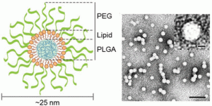
The synthesis of nanoprobes for application in more than one imaging technology is becoming more popular. So-called “bi-modal” probes can reduce limitations of single imaging modalities such as sensitivity or penetration depth. In this Hot article, the synthesis of two amphiphilic, dual-modality, optical imaging/MRI nanoprobes is reported. Each probe, containing both a fluorophore and a gadolinium complex, was specifically engineered using hydrophobic and hydrophilic components so they would self-assemble above the critical micelle concentration (CMC), which in turn would improve the MRI performance. The materials could offer potential advantages compared to conventional, unimolecular probes. Flow cytometry was used to confirm that both negatively charged assemblies were efficient at labelling KB-3-1 (human cervical cancer) cells at different labelling concentrations and incubation periods, through measurement of cell fluorescence. Cells viability was not compromised for each condition. The authors are now looking to further improve performance of self-assembled cell tracking agents through synthetic manipulation of construct size and surface charge.

Design and assembly of supramolecular dual-modality nanoprobes
Shuang Liu, Pengcheng Zhang, Sangeeta Ray Banerjee, Jiadi Xu, Martin G. Pomper and Honggang Cui
Nanoscale, 2015, 7, 9462-9466. DOI: 10.1039/C5NR01518A

Dr Mike Barrow is a guest web writer for the Nanoscale blog. He currently works as a Postdoctoral Researcher at the University of Liverpool.

Digg This
Reddit This
Stumble Now!
Share on Facebook
Bookmark this on Delicious
Share on LinkedIn
Bookmark this on Technorati
Post on Twitter
Google Buzz (aka. Google Reader)

Ready. Set. GO!

Written by Dr Lee Barrett.

Graphene oxide (GO) is a versatile material with applications ranging from electronics to energy storage and biosensors. As a biosensing substrate, GO has many favorable attributes such as low cost, high signal-to-noise ratio, and the ability to efficiently quench fluorescence.

Scheme for the GO-aptamer based sensor for detection of thrombin.

This ability to quench fluorescence has inspired a range of biosensors using GO and Förster resonance energy transfer (FRET) for the sensitive detection of proteins using labelled probes, such as aptamers. However, the target proteins in such assays can non-specifically adsorb onto the surface of GO, thereby reducing the sensitivity.

To address this, Gao and co-workers implemented the use of polyethylene glycol (PEG) to prevent the non-specific adsorption of thrombin onto GO while implementing an aptamer-binding assay.  The authors report that the detection limit could be improved by optimizing the GO:PEG concentration. This manuscript helps to establish GO as promising tool in the biomedical and biotechnology fields.

Highly sensitive detection for proteins using graphene oxide-aptamer based sensors
Li Gao, Qin Li, Raoqi Li, Lirong Yan, Yang Zhou, Keping Chen and Haixia Shi
Nanoscale, 2015, Advance Article. DOI: 10.1039/C5NR01187F

Dr Lee Barrett is a guest web writer for the Nanoscale blog. Lee is currently a postdoctoral researcher in the Centre for Molecular Nanometrology at the University of Strathclyde. His research is currently focused on the development of nanoparticle-based sensors and surface enhanced Raman scattering (SERS). Follow him on Twitter @L_Bargie.

Digg This
Reddit This
Stumble Now!
Share on Facebook
Bookmark this on Delicious
Share on LinkedIn
Bookmark this on Technorati
Post on Twitter
Google Buzz (aka. Google Reader)

HOT article: Two-dimensional materials and their prospects in transistor electronics

Written by Sebastian Axmann.

Recently, the 50th anniversary of Moore’s law has been celebrated by the semiconductor industry. Although the current ITRS (International Technology Roadmap for Semiconductors) continues to propose “traditional” transistor materials such as Si and GaAs, attractive, two-dimensional alternatives have become visible on the horizon.

Schwierz et al. have recently published a Feature article in Nanoscale compiling the current knowledge on 2D materials. Their article focuses on the application of these as the channel material in field effect transistors.

According to the authors, two large trends can currently be observed: More Moore and More than Moore. The former utilizes well known semiconductors and improves performance by sophisticated manufacturing and scaling techniques. In contrast, the latter one employs compound semiconductors and novel alloys as 2D materials with a wide range of new properties.

Two-dimensional materials and their prospects in transistor electronics

The main material classes researched to date are explained further, covering X-anes, Fluoro-X-enes, TMDs (transition metal–chalcogen combinations), SMCs (semimetal–chalcogen combinations), MX-enes and (currently theoretical) group IV-IV and III-V 2D materials.

To assess the viability of the materials for applications within electronic circuits, Schwierz et al. also describe a wish list of ideal properties of next generation channel materials: bandgap, carrier mobility, heat conductivity, contact resistance and scale length. Based on experiences from established semiconductors, they also derive practical values needed for high performance FET.

The final part of the review examines the current status of the material classes. Notable performance records of well researched materials (e.g. 100 GHz graphene FET) as well as first demonstrators (e.g. first X-ane based FET) are given here. Finally, some arguments for a revival of silicon as a promising material for future applications are also given.

Two-dimensional materials and their prospects in transistor electronics
F. Schwierz, J. Pezoldt and R. Granzner
Nanoscale, 2015, 7, 8261-8283. DOI: 10.1039/C5NR01052G

Sebastian Axmann is a guest web-writer for the Nanoscale blog. His interests comprise manufacturing and metrology of nanostructures as well as their usage in current semiconductor devices. He also posts links to interesting research articles on Twitter: @SebastianAxmann.

Digg This
Reddit This
Stumble Now!
Share on Facebook
Bookmark this on Delicious
Share on LinkedIn
Bookmark this on Technorati
Post on Twitter
Google Buzz (aka. Google Reader)

HOT article: Photo-fluorescent and magnetic properties of iron oxide nanoparticles for biomedical applications

Written by Dr Derek Craig.

As cancer treatments evolve, focus has shifted to techniques and tools, which provide tumor-targeting capabilities and are uncoupled from common detrimental side effects.  The efficient delivery of new therapeutics has been a common area of interest, with studies focused on nanoparticle delivery systems being an eminent research area.

(a) TEM image of PS/Fe3O4 microspheres showing the amorphous coating entrapping multiple Fe3O4 nuclei. (b) TEM image of PAA/Fe3O4 and (c) cumulant size distribution of PAA/Fe3O4.

In this review article, Shi and co-workers draw attention to the properties of magnetite nanoparticles (Fe3O4), which can be utilised as customized therapeutics.  This review provides an overview of the synthesis of magnetite nanoparticles with an in-depth discussion related to their synthesis, functionalization and applications in a biological environment.

A highlight of this review includes an exploration into the recently discovered photo-luminescence properties of magnetite nanoparticles through studies of the electronic band structures to explain the emission mechanisms occurring.  The implications of thermal and magnetic induced hypothermia treatments utilizing these nanoparticles are also discussed relative to the patients being treated by such techniques.

From this review it can be determined that a new theragnostic platform has emerged with multi-functional capabilities both in terms of imaging and drug delivery.

Photo-fluorescent and magnetic properties of iron oxide nanoparticles for biomedical applications
Donglu Shi, M. E. Sadat, Andrew W. Dunn and David B. Mast
Nanoscale, 2015, 7, 8209-8232. DOI: 10.1039/C5NR01538C

Dr Derek Craig is a guest web writer for the Nanoscale blog. He is a Post Doctoral Research Fellow at the University of St. Andrews based in the fields of Biophotonics and Materials Science. With a background in chemistry, his work mainly focuses on the synthesis of nano to meso materials and the use of imaging techniques to study biological samples.

Digg This
Reddit This
Stumble Now!
Share on Facebook
Bookmark this on Delicious
Share on LinkedIn
Bookmark this on Technorati
Post on Twitter
Google Buzz (aka. Google Reader)

Single-walled carbon nanotubes: Catching some rays

Written by Dr Lee Barrett.

Precision printing and optical modeling of ultrathin SWCNT/C60 heterojunction solar cells

Inexpensive photovoltaics (PV) are an attractive avenue of research in the field of solar cells. In particular, semi-conducting single-walled carbon nanotubes  (s-SWCNTs) are a promising photo-absorbing material due to their strong near-infrared (near-IR) absorption and high carrier mobility. However, most current production methods for SWCNT PVs suffer from high surface roughness and lack nanometer-scale deposition precision, thereby hampering the reproducibility of ultrathin PV devices.

To this end, the authors have utilized ultrasonic spraying in order to tune the thickness of s-SWCNT layers with nanometer-scale precision. The researchers have used a combination of atomic force microscopy (AFM) and optical profilometry to show that their ultrasonic spraying method produces smooth, uniform films with an average roughness of about 5 nm.  The advantage of this low roughness enables fabrication of s-SWCT/C60 bilayer devices with significantly thinner C60 layers than previously reported.

The results reported by the authors help to advance the production of low-cost PV devices by improving the performance and scalability of ultra-thin SWCNT-based solar cells. Ultra-thin SWCNTs reported here could find potential use in other emerging technologies such as vertical field effect transistors and light-emitting diodes incorporating s-SWCNT injection layers.

Precision printing and optical modeling of ultrathin SWCNT/C60 heterojunction solar cells
Sarah L. Guillot, Kevin S. Mistry, Azure D. Avery, Jonah Richard, Anne-Marie Dowgiallo, Paul F. Ndione, Jao van de Lagemaat, Matthew O. Reese and Jeffrey L. Blackburn
Nanoscale, 2015, 7, 6556-6566. DOI: 10.1039/C5NR00205B

Dr Lee Barrett is a guest web writer for the Nanoscale blog. Lee is currently a postdoctoral researcher in the Centre for Molecular Nanometrology at the University of Strathclyde. His research is currently focused on the development of nanoparticle-based sensors and surface enhanced Raman scattering (SERS). Follow him on Twitter: @L_Bargie.

Digg This
Reddit This
Stumble Now!
Share on Facebook
Bookmark this on Delicious
Share on LinkedIn
Bookmark this on Technorati
Post on Twitter
Google Buzz (aka. Google Reader)