Author Archive

Transparent nanopaper for the next generation of renewable, flexible electronics

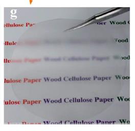
The next generation of flexible electronic devices will use transparent nanopaper, a flexible, renewable and tunable substrate that can be used in thin film resistors, organic light emitting diodes and organic photovoltaics.

Hybrid NFC nanopaper

Renewable, flexible paper electronics have been a tantalizing prospect for quite a while, yet they suffered from significant flaws including large surface roughness and high opacity.  New techniques have been developed to extract what is known as nanofibril cellulose (NFC) from natural wood fibers.  The paper that can be made from NFC has high transparency, extremely low surface roughness and good mechanical properties.  This review article covers fabrication techniques for nanopaper, optical and mechanical properties of the nanopaper, and devices constructed using electronics on transparent nanopaper.

While researchers are still working to develop high throughput, low energy fabrication techniques for nanopapers, the currently developed techniques have already yielded paper with exciting properties.  The optical transparency of the nanopaper can be as high as 90%, and the amount of haze can be tuned to optimize for a variety of applications.  High haze is ideal for light scattering in photovoltaics and in screens for outdoor viewing, while low haze is optimal for high clarity screens for indoor viewing.  Nanopaper also has extremely low surface roughness (5 nm), high mechanical strength and low thermal expansion.

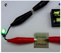
Organic LED made using transparent nanopaper

These physical and optical properties make nanopaper an ideal medium for the next generation of flexible electronics.  When coated with a conductive layer such as ITO, carbon nanotubes or silver nanowires, the conductivity of the nanopaper is high enough to allow it to be used in thin film transistors and organic LEDs.  Though not yet as efficient as plastic substrates, nanopaper can also be used to make organic photovoltaics with much higher efficiencies than those with paper substrates.  Finally, researchers have created a resistive touch screen from nanopaper – one that outperforms PET (polyethylene terephthalate) in sunny conditions.

Want to know more?  Check out the full article in EES today!

Transparent paper: fabrications, properties, and device applications

Hongli Zhu, Zhiqiang Fang, Colin Preston, Yuanyuan Li and Liangbing Hu

DOI: 10.1039/c3ee43024c

Digg This
Reddit This
Stumble Now!
Share on Facebook
Bookmark this on Delicious
Share on LinkedIn
Bookmark this on Technorati
Post on Twitter
Google Buzz (aka. Google Reader)

Advancing Solar Energy: High-Efficiency Silicon Solar Microcells

Schematic of silicon solar microcell fabrication process and SEM and optical microscope images of fabricated cells

A) Microcell design B) Microcell fabrication scheme C)SEM of fabricated microcells D) optical image of microcell array

While silicon solar panels corner a large part of the current solar energy market, they are still too expensive to compete directly with fossil fuels.  However, new advances in silicon solar microcells bring increases in process reliability, efficiency and cost, making solar energy more scalable and affordable.

In their recent paper, Yao et. al demonstrate a redesigned silicon solar µ-cell which incorporates a thermal oxide as a robust etching and diffusion mask, which also serves as an anti-reflection and surface passivation coating.  They also put forth design criteria optimizing the spatial distribution of µ-cells to maximize light-trapping and for the integration of backside reflectors and polymer waveguides into devices for optimal performance.

The figures of merit for the champion device are an open-circuit voltage of 0.534 V, a short-circuit current density of 28.7 mA cm-2, a fill-factor of 0.762 and an overall efficiency of 11.7%.  Interestingly, they demonstrate the efficacy of the thermal oxide as a passivation layer by testing a device before and after the oxide is etched off, showing that removing the oxide causes a significant decrease in performance.  They also show that the incorporation of backside reflectors and planarization layers significantly enhances device performance.

An important consideration for any emerging solar energy technology is scalability.  These redesigned silicon solar µ-cells have a peak-power-generation referenced silicon consumption of only 0.4 g Wp-1, substantially lower than the 10 g Wp-1 of commercially available silicon solar cells.  Combined with the scalability of the processing steps used in the µ-cell fabrication, the low amount of silicon required could be a huge step forward in reducing the cost of solar energy.

Excited about new advances in renewable energy?  Read this full article and many more in EES today!

Fabrication and assembly of ultrathin high-efficiencysilicon solar microcells integrating electrical passivation and anti-reflection coatings
Yuan Yao, Eric Brueckner, Lanfang Lib and Ralph Nuzzo
DOI:10.1039/C3EE42230E

Digg This
Reddit This
Stumble Now!
Share on Facebook
Bookmark this on Delicious
Share on LinkedIn
Bookmark this on Technorati
Post on Twitter
Google Buzz (aka. Google Reader)