Magnets for facile molding of via holes in PDMS

Corey Koch and co-workers describe the use of magnetic molds for construction of complex PDMS devices

Corey Koch, James Ingle, and Vincent Remcho
Department of Chemistry, Oregon State University, Corvallis, Oregon, USA

Why is this useful?


The formation of vias between microchannels in PDMS and fluidic interconnects is commonly performed by using a punch to cut away PDMS. This process often results in a torn surface that is not as resilient to pressure driven flow, can create material that clogs channels, provides less control of hole shape, and results in the formation of irregular surfaces that increase dead volume.[1] A smoother surface finish and more controllable hole geometries have been achieved by using posts in the molding process.[2] Magnetic fixturing of via holes provides a readily configurable and facile means to locate and hold posts. Magnets also come in all shapes and sizes and can therefore provide a creative means to incorporate mesoscale features into PDMS microchips. In this example, cylindrical neodymium magnets are used to mold via holes into a PDMS microchip.

What do I need?


  • Magnets for molding. Neodymium magnets provide the strongest field and are available commercially in a variety of shapes and sizes.
  • A microchip master mold. Guide features on the microchip master can aid magnet alignment.
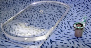
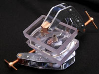
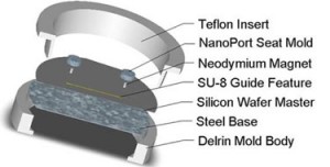
  • A PDMS molding fixture that can attract magnets. A mold made from a ferromagnetic material (such as steel) or placing a magnetic base below a plastic or aluminum fixture, as shown in Figure 1, can provide a means to hold the magnets.
  • PDMS (Dow Corning Sylgard 184).
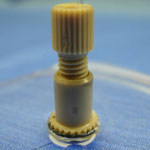
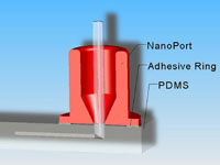
  • In this example, a flat surface was necessary above the via hole to bond Upchurch NanoPorts as interconnects. Because PDMS forms a meniscus on the surface around the magnet when curing, a steel cylinder was placed above the via hole molding magnet to create a NanoPort mating seat.
    Figure 1

What do I do?


1.  Prepare your master mold, magnetic PDMS mold (An SU-8 on silicon microchip master mold and steel base are shown as an example in Figure 2), and your magnets.

Figure 2

2.  Place the magnets on the appropriate guide features on the master mold as shown in Figure 3. In this example 1/8″ high by 1/16″ diameter cylindrical magnets and a specially designed plastic mold with a steel base (as shown in Figure 1) were used. An aluminum foil mold as described in “Chips and Tips: Rapid curing of PDMS for microfluidic applications” could be used for a quick and easy molding platform.

Figure 3

3.  In this example a flat surface is needed for bonding Upchurch NanoPorts, so a steel cylinder (Figure 4) with a diameter greater than the NanoPort is placed on top of the magnet to move the PDMS meniscus away from the center of the via hole and provide a flat seat for bonding.

Figure 4

4.  Pour the PDMS as shown in Figure 5 (mixed to manufacturer specifications or for your specialty application). Bubbles can get trapped under the steel ‘NanoPort seat’ so fill the mold slowly or degas after filling.

Figure 5

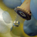
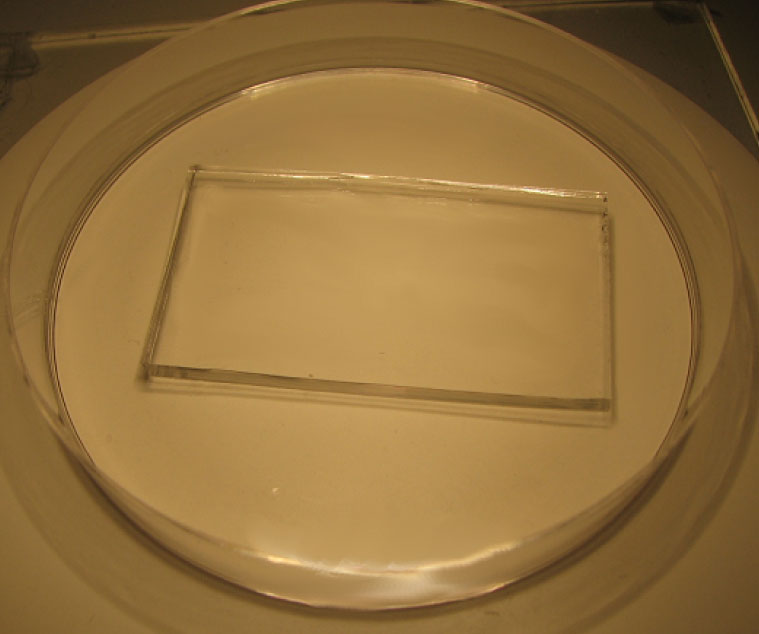
5.  Cure the PDMS at your desired temperature. Remove the PDMS from the mold and use a tweezers to pull out the magnet. Cut the chip to size as shown in Figure 6 and notice the quality of your now ready via hole!

Figure 6

6.  In this example, the steel ‘NanoPort seat’ provided a flat surface to bond the NanoPort, and the meniscus actually allows for rapid registration of the NanoPort to the via hole (Figure 7). The 1/8″ high by 1/16″ diameter magnets used can be placed close enough for maximum NanoPort packing density (magnets within 5 mm of each other).

Figure 7

Using magnetic posts can provide a variety of shapes and sizes of via holes, a smooth hole, and a convenient method for securing posts during molding.

Another quick tip for using 1/16″ tubing: employ 1/16″ diameter cylindrical magnets and tubing with a small ID. Cut the tubing at a slight angle and insert it to the bottom of the via hole to minimize dead volumes in your interconnect.

Acknowledgements


This material is based upon work supported by the National Science Foundation under Grant No. DGE-0549503. This research was also supported by a research grant from the U.S. Environmental Protection Agency sponsored Western Region Hazardous Substance Research Center under agreement R-828772. This work has not been reviewed by the agency, and no official endorsement should be inferred. We would like to recognize Ted Hinke at the Oregon State University Department of Chemistry Machine shop for his help in mold design and his skill in its construction.

References


1] S. Li and S. Chen, IEEE Transactions on Advanced Packaging200326, 242-247.
[2] D. C. Duffy, J. C. McDonald, O. J. A. Schueller and G. M. Whitesides, Anal. Chem.199870, 4974-4984.

Digg This
Reddit This
Stumble Now!
Share on Facebook
Bookmark this on Delicious
Share on LinkedIn
Bookmark this on Technorati
Post on Twitter
Google Buzz (aka. Google Reader)

A foolproof method for enclosing glass-based LOC devices for electrophoresis

Colin Mansfield and co-workers describe a simple method to produce a leak free and easily reusable device for electrophoresis.

Colin D. Mansfield, Radoslaw Mazurczyk and Julien Vieillard
Institut des Nanotechnologies de Lyon, Ecole Centrale de Lyon, France

Why is this useful?


Bonding of glass-based lab-on-a-chip (LOC) devices presents a challenging, time-consuming problem, often requiring specialist equipment and skills. Moreover, it is fraught with dangers that if the typically elaborate protocol [1-3] is not strictly followed, then the chip’s channels may leak, ruining an otherwise perfectly good device. Ironically, successful bonding can also be a liability, a chip’s lifetime being reduced due to the difficulties and ambiguity associated with thoroughly cleaning its channels between experiments. Other factors that make bonding of glass-based microdevices problematic include: (i) the inherent nanometre roughness of glass (which renders direct glass-glass bonding a non-trivial task); (ii) low-temperature requirements imposed by possible integration of opto-electronic components; (iii) certain processes, (e.g. ion-exchange waveguide integration) can introduce surface defects (~200 nm in height) that preclude any possibility of glass-to-glass bonding without planarization.

This tip describes a simple, inexpensive and reversible solution to enclose microchannels, using a sheet of polydimethylsiloxane (PDMS). It avoids all the pitfalls mentioned; the natural compliance and adhesion of the PDMS sheet conforms efficiently to the glass substrate’s topography to form a leak-free seal, while the ‘bonding’ is performed at room temperature with very basic equipment. Moreover, since the PDMS layer is easily peeled away from the substrate, there are no consequences if the initial alignment fails and there is full access to the microchannels during cleaning, allowing chips to be recycled.

What do I need?


  • Sylgard 184 silicone elastomer kit (DowCorning).
  • Flat glass support, preferably with raised edges.
  • Measuring cylinder, beaker, plastic stirrer, xylene, paper towels.
  • Cutter, ruler, print-off of device geometry, hole punch, tweezers.
  • Oven, spin-coater (optional).Mix PDMS and curing agent in a 10:1 weight ratio in a disposable weigh boat.

What do I do?


1.  PDMS is messy stuff, so first cover the working area with paper towels to catch any spills.

2.  Mix the base polymer and curing agent in a ratio of 10:1 and stir vigorously for 5 minutes to obtain a homogeneous solution. (For a 15 x 15 cm glass support, approximately 16.5 ml and 55 ml total volume produces sheets of thickness 0.75 mm and 2.5 mm respectively).

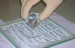
3.Pour this mixture evenly onto the glass support and let it rest for 1 hour to degas and flow (Figure 1). (This process can be accelerated by placing it into a ultrasonic bath for 5 min before pouring).

Figure 1. Degassed PDMS mixture being poured onto glass support.

4.  Place the glass support onto a flat surface in the oven and bake for 1 hour at 100 °C. (Alternatively, 24 hours at room temperature or 30 min at 120°C also work well).

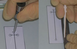
5.  Once cooled, place the glass support over your template and scribe around the LOC’s perimeter. If access ports are required, use the punch (e.g. 2 mm outer diameter) to cut out  holes, taking care not to leave any shreds (Figure 2).

Figure 2. PDMS being shaped to LOC geometry.

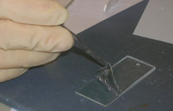
6.  Remove the PDMS cover with plastic tweezers and place it over your prepared LOC (Figure 3), ensuring that the side in contact with the support’s surface is face-down. Any trapped air is easily expelled by applying light pressure to the PDMS and pushing it towards the edge. If you are unhappy with the final alignment or cannot remove some trapped air, simply peel off the PDMS layer and repeat this step.

Figure 3. Application of PDMS cover to glass LOC.

7.  For clean-up of PDMS pre-polymer liquid, we have found the solvent xylene works well.

What else should I know?


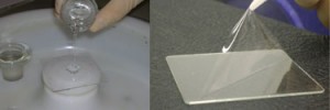
Since it is simple to control the thickness of the PDMS sheet it is also possible to fabricate ‘windows’ of < 50 µm thickness, thereby enclosing the channel and also allowing a delivery/collection fibre to be positioned in very close proximity to the microchannel [4]. The protocol is as described above, however, there is no need for degassing and the layer is prepared using a spin-coating method (1500 rpm, 40 s) onto a glass slide (6 x 6 cm) (Figure 4).

Figure 4. Spin coating of a thin (< 50 µm) PDMS sheet.

Based upon a PDMS cover of 75 x 25 x 0.75 mm, we estimate the cost of this method to be less than 15 pence/device. This may be especially beneficial to teaching establishments that can use a small number of glass etched devices many times over for practical courses. Although this approach has proven viable in electrophoretic studies,[4] it does have some limitations. Namely, (i) plug flow will be distorted at the glass/PDMS interface, deteriorating separation performance and (ii) proteins are prone to adsorption by the PDMS, worsening the resolution of electrophoresis and hindering the detection of trace proteins. The good news is however, that if data acquired using such a hybrid device shows any signs of promise, your efforts in fabricating a fully glass-bonded chip are certain to be rewarded.

Acknowledgements


Colin Mansfield acknowledges the financial support of the European Community under a Marie Curie Intra-European Fellowship, administered by Dr S Krawczyk.

References


[1] A. Iles, A. Oki and N. Pamme, Bonding of soda-lime glass microchips at low temperature. Microfluid. Nanofluid., 2007, 3, 119-122.
[2] L. Chen, G. Luo, K. Liu, J. Ma, B. Yao, Y. Yan and Y. Wang, Bonding of glass-based microfluidic chips at low- or room-temperature in routine laboratory, Sens. Actuators, B, 2006, 119, 335-344.
[3] N. Chiem, L. Lockyear-Shultz, P. Andersson, C. Skinner and D. Jed Harrison, Room temperature bonding of micromachined glass devices for capillary electrophoresis. Sens. Actuators, B, 2000, 63, 147-152.
[4] R. Mazurczyk, J. Vieillard, A. Bouchard, B. Hannes, S. Krawczyk, A novel concept of the integrated fluorescence detection system and its application in a lab-on-a-chip microdevice. Sens. Actuators B, 2006, 118, 11-19.

Digg This
Reddit This
Stumble Now!
Share on Facebook
Bookmark this on Delicious
Share on LinkedIn
Bookmark this on Technorati
Post on Twitter
Google Buzz (aka. Google Reader)

Organic solvent compatible reservoirs for glass microfluidic chips

Michael Watson and Aaron Wheeler describe an alternative to using non-solvent resistant adhesives to attach reservoirs to microfluidic chips.

Michael W. L. Watson and Aaron R. Wheeler
Department of Chemistry, University of Toronto, Ontario, Canada

Why is this useful?


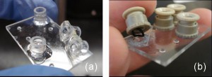
Some applications for microfluidics, such as synthesis, reversed phase separations, and liquid-liquid extraction, require the use of organic solvents (e.g. acetonitrile, methanol, etc.).  For such applications, glass or quartz substrates are preferred; however, even when using solvent-resistant substrates, such applications are often limited by the problem of connecting reservoirs to the substrate. As illustrated in Figure 1, common adhesives used for this purpose, such as epoxies and UV cured glues, are not able to withstand extended periods of exposure to solutions with high organic solvent content.

Figure 1: Reservoirs connected with traditional adhesives

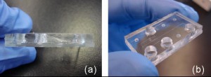
In this Tip, we report a straightforward solution to this problem: using an oxygen plasma bonded poly(dimethyl siloxane) (PDMS) reservoir manifold (Figure 2).

Figure 2: An organic solvent compatible reservoir

This structure is inexpensive, easy to apply, and is able to withstand a wide range of organic solvents for periods of up to several weeks.

What do I need?


  • PDMS.   We use the Sylgard 184 PDMS kit   (Dow Corning Company), but any of a variety of PDMS formulations could be used.
  • Vacuum chamber.   An air-tight chamber that can be attached to a pump or house vacuum.   We use a vacuum oven (Fisher Scientific Model 280A).
  • Oven.   PDMS can be cured at room temperature overnight, but the process is much faster in an oven.
  • Plasma cleaner.   We use a Harrick Plasma cleaner (Model PDC-001) to pre-treat glass and PDMS surfaces prior to bonding.   An air plasma can be used but an oxygen plasma will yield a better seal.
  • Glass microfluidic chip. Home-made or purchased glass or quartz microfluidic devices are required for work with strong organic solvents. We purchase chips from Caliper Life Sciences.
  • Hole punch or coring tool. The reservoir volume is determined by the diameter of the holes in the manifold.   We use either a coring tool with a diameter of 2 mm or a paper hole punch with a diameter of 5 mm.

What do I do?


  1. Mix PDMS and curing agent in a 10:1 weight ratio in a disposable weigh boat.
  2. Degas PDMS under vacuum.
  3. Pour the PDMS into a plastic Petri dish to a depth of about 3-4 mm.
  4. Cure PDMS for 1 hour at 70oC.
  5. Cut the PDMS with a scalpel to fit the shape of the microfluidic device.
  6. Punch holes through the PDMS such that they line up with the inlet ports in the microfluidic device. (For alignment, fit the PDMS manifold to the glass surface and use a Sharpie to mark the locations of the holes, prior to bonding, test-fit the manifold to ensure that the punched holes align with the microfluidic inlet ports.)
  7. Clean the glass device and manifold with deionized water and isopropanol and dry under a stream of nitrogen.
  8. Plasma treat the surfaces to be bonded under oxygen (5 psi O2, 400 mtorr vacuum, 26.9 W, 90 s).
  9. Bring the two surfaces together.  Press down firmly for 20-30 s to ensure good seal formation.
  10. After use, the glass chip can be recycled by removing the PDMS slab with a razor blade and cleaning with acetone.
What else should I know?


These reservoirs provide a transparent alternative to opaque adhesives making it easier to visualize networks of channels and use optical detection methods. While some swelling is observed in solvents such as acetonitrile, the seal between the PDMS and glass does not leak, allowing for weeks of continued exposure to organic solvents. Note that highly aggressive solvents such as ethers or benzene are not compatible with this method.

Digg This
Reddit This
Stumble Now!
Share on Facebook
Bookmark this on Delicious
Share on LinkedIn
Bookmark this on Technorati
Post on Twitter
Google Buzz (aka. Google Reader)

Preventing suspension settling during injection

Ryan Cooper and Luke Lee describe how to avoid settling of suspensions during injection onto a chip.

Ryan Cooper and Luke Lee
Department of Bioengineering, University of California-Berkeley, Berkeley, California

Why is this useful?


This technique was developed to solve the problem of cell suspensions settling to the bottom of the syringe during the time it took to load them into a device. It is a gentle method to keep mixtures of cells, beads and other particles in suspension.

What do I need?


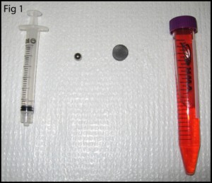
  • 1 Loading Syringe
  • 1 Stainless Steel Ball Bearing (recommended diameter 1/3 to 2/3 the inside diameter of the syringe)
  • 1 Magnet

What do I do?


1. Clean the ball bearing with acetone followed by alcohol to remove any grease and sterilize its surface.

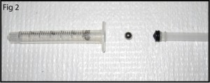
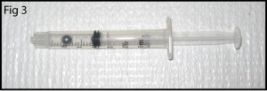
2. Pull the plunger out of the syringe (in a clean hood if sterile conditions are required) and drop the ball bearing into the tube, then reinsert the plunger (Fig. 2, Fig. 3).

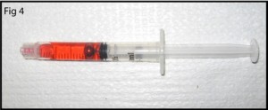
3. Fill the syringe part way with the desired solution (Fig. 4)

4. Hold the syringe upright and tap its side to make the air bubbles inside float to the top of the syringe, then force them out with the plunger.

5. Once the air bubbles are out, finish filling the syringe (Fig. 5).

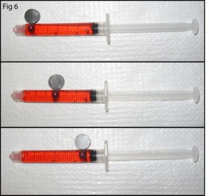
6. To prevent the solution inside the syringe from settling, simply move the magnet back and forth across the surface of the syringe, dragging the ball bearing back and forth inside the syringe and agitating the solution (Fig. 6).

7. Now you can take as long as you need to load the solution since you can prevent settling. If you do not have a magnet, the solution can be agitated by tipping the syringe and using gravity to move the bearing. Placing the entire syringe pump on a rocker plate could also be employed to move the bearing.

Digg This
Reddit This
Stumble Now!
Share on Facebook
Bookmark this on Delicious
Share on LinkedIn
Bookmark this on Technorati
Post on Twitter
Google Buzz (aka. Google Reader)

Quick and cheap syringe-tubing interfacing

Rodrigo Martinez-Duarte and Marc Madou describe a simple method to connect syringes to chips.

Rodrigo Martinez-Duarte and Marc Madou
BioMEMS Research Laboratory, Department of Mechanical & Aerospace Engineering, University of California, Irvine. Irvine, CA.

Why is this useful?


This tip describes an easy, quick and cheap way to interface syringes to 1/16″ OD (outer diameter) tubing for low and medium pressure applications.  This methodology allows for very quick fabrication with off-the-shelf components as well as modularity since connectors can be easily swapped to other syringes, in contrast to some connecting methods which require connector fabrication for each syringe used.  The connector is very easy to use.

We use 1/16″ OD tubing since many compatible parts such as Y connectors, valves and others are available through online vendors (e.g., Upchurch).

What do I need?


  • 1/16″ OD tubing. A wide variety of tubing materials and sizes are available from Upchurch.  In particular we have used Teflon tubing (catalog number 1620). You could also find the connector at Upchurch (TEFZEL, catalog number P-870)
  • Female Luer to 1/16″ ID (inside diameter) Barbed connector, shown in Fig. 1. A wide choice of materials for connectors are available from Gosina.
  • 3M  Polyolefin Heat Shrink (HS) Tubing 3/64″. Although we have used 3M tubing (Polyolefin Heat Shrink Tubing 3/64″) heat shrink tubing with ID of 1/16″ should work as well. HS tubing is available from a number of suppliers including Fisher.
  • Heating element. A soldering iron would be the most common heating element. You can get a basic one from Fisher (catalog number S50350).

Figure 1. Barbed to female luer connector

What do I do?


1. Wear gloves before starting. You don’t want to introduce impurities during fabrication that could contaminate your device channel in future experiments.
2. Cut around 1 cm of HS tubing.
3. Cut desired length of 1/16″ OD tubing. (If you don’t have a special cutter, use scissors instead of knife to assure a cleaner cut.)
4. Sterilize all components with isopropanol for 2-3 minutes then blow dry.
5. Take the HS tubing. Insert one end to the barbed side of the connector. Make sure tubing is  inserted all the way to the base of the connector (~5 mm).
6. On the other end insert the 1/16″ OD tubing. Insert for around 2-3 mm.
7. Leave around 2 mm of HS tubing length between the barbed connector and the 1/16″ OD tubing; it will allow you to have up to 90 degree angles between your tubing and the syringe since once HS tubing is heat shrunk it will be very flexible.
8. Using the heating element, apply heat along all the HS tubing. Connections will further seal as tubing shrinks. Do not apply too much heat or you might melt the 1/16″ OD tubing or the connector.
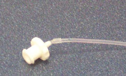
9. The finished connector is shown in Figure 2.

Figure 2. Completed connector

What else should I know?


These connectors have been tested with DI water, alcohol, yeast samples, diluted YPD growth medium, air and sodium dodecyl sulfate with reliable performance.

The connector can be dismantled by just pulling components apart. The barbed connectors and 1/16″ OD tubing are not damaged and can be reused.

Digg This
Reddit This
Stumble Now!
Share on Facebook
Bookmark this on Delicious
Share on LinkedIn
Bookmark this on Technorati
Post on Twitter
Google Buzz (aka. Google Reader)

On-chip electrophoresis devices: do’s, don’ts and dooms

Juan Santiago and co-workers provide some simple rules of thumb for success in on-chip electrophoresis

Alexandre Persat, Tom Zangle, Jonathan Posner and Juan Santiago
Stanford Microfluidics Laboratory, Department of Mechanical Engineering, Stanford University, Stanford, CA

Background


On-chip electrokinetic injections and on-chip electrophoresis are well-established techniques, and the field is about 15 years old [1].The techniques for on-chip sample loading, voltage control, injection, separation, visualization, and electropherogram detection have been described in numerous publications [2, 3]; a few of these are summarized by Sharp et al. [4].

Below we present a few informal “tips” listed under various categories that we hope may be useful to new users of this technology.  These instructions are in no way comprehensive, are not even quantitative, but we hope they will save someone somewhere some time.

References


1. A. Manz, D. J. Harrison, E. M. J. Verpoorte, J. C. Fettinger, A. Paulus, H. Ludi and H. M. Widmer, J. Chromatogr., 1992, 593(1-2), 253-258.
2. A. Manz, C. S. Effenhauser, N. Burggraf, D. J. Harrison, K. Seiler and K. Fluri, J. Micromech. Microeng., 1994, 4(4), 257-265.
3. G. J. M. Bruin, Electrophoresis, 2000, 21(18), 3931-3951.
4. K. V. Sharp, R. J. Adrian, J. G. Santiago and J. I. Molho, “Liquid Flows in Microchannels” (updated), in CRC Handbook of MEMS, CRC Press, 2006, Boca Raton, Florida, USA.

Digg This
Reddit This
Stumble Now!
Share on Facebook
Bookmark this on Delicious
Share on LinkedIn
Bookmark this on Technorati
Post on Twitter
Google Buzz (aka. Google Reader)

Rapid prototyping of microfluidics

Richard Holmes and Nicholas Goddard describe rapid prototyping of microfluidic systems using double sided tape.

Richard J. Holmes and Nicholas J. Goddard
School of Chemical Engineering and Analytical Science (SCEAS),The University of Manchester, Manchester, UK

Why is this useful?


We demonstrate the use of double-sided adhesive films in the development of rapid prototype flow systems. These prototype fluidic devices have a great number of applications and since their preparation is a trivial matter, they may be prepared as and when required. Where there is a requirement for fluidic systems with a greater depth than the thickness of the film, multiple layers may be employed to expand the range of device depths obtainable.

What do I need?


  • ARCare 8725 double-sided adhesive (or similar)
  • Craft Knife, cutting board, template/ruler, etc.
  • Polycarbonate (or glass) slides with appropriately located inlet and outlet holes.

What do I do?


1. First, prepare the substrate and superstrate, cleaning both and locating any inlet and outlet connectors and / or holes as appropriate.

2. Prepare a template of the channel design required and transfer this to the backing tape of the adhesive film.

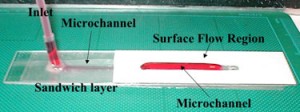
Figure 1. Sandwich-structure microfluidic device, illustrating internal and external flow control structures

3. Cut the adhesive film using the sharp craft knife, removing all traces of the template drawing, thereby leaving a double-sided adhesive film with missing segments corresponding to the desired flow system.

4. Adhere the film to the underside of the superstrate ensuring access to the inlet and outlet wells.

5. Remove the backing tape and attach the substrate slide, applying pressure to the system to assist adhesion process, creating a sandwich structure where the adhesive film defines the microfluidic system.

Figure 2. Sandwich-structure microfluidic device, filled with amaranth dye solution, enhancing the contrast of the internal and external flow control structures from the polycarbonate body of the device

The device shown in the Figures 1 and 2 combines an internal flow system with an external flow system, using multiple layers of the adhesive tape to define a flow profile on the upper surface of the chip, whilst maintaining fluid confinement.

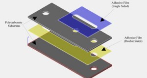
Figure 3. A cross-section of the device shown in Figures 1 & 2. Single- and double-sided adhesives can be used with polycarbonate slides to build multi-layer devices

Figure 3 shows a cross-section of the device. This system may also be utilised for the formation of devices where the channel is pre-defined in either the substrate or the superstrate, as shown in Figure 4.

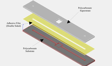
Figure 4. Sandwich-structure consisting of two polycarbonate slides, bonded using ARCare 8725 adhesive tape; microfluidic system defined in polycarbonate slide by CNC milling.

Figure 5 shows a cross-section of the device.

Figure 5. A cross-section of the device shown in Figure 4

What else should I know?


The method presented above is a useful technique in the preparation of flow systems for microfluidics work on a prototype scale. Whilst the limitations of the system are obvious in so far as pressure driven systems, where high pressure flow will result in rupture of the device, and the use of a silicon-based adhesive limits the applications for any systems requiring abrasive chemical or surface chemistry, it does provide ample opportunity to demonstrate a flow system, producing a working model in a very short space of time.

Digg This
Reddit This
Stumble Now!
Share on Facebook
Bookmark this on Delicious
Share on LinkedIn
Bookmark this on Technorati
Post on Twitter
Google Buzz (aka. Google Reader)

Superior data presentation of poor quality microfluidics images

Richard Holmes and Nicholas Goddard describe a simple method to manipulate video images of microfluidics for presentation in print.

Richard J. Holmes and Nicholas J. Goddard
School of Chemical Engineering and Analytical Science (SCEAS),The University of Manchester, Manchester, UK

Why is this useful?


A number of journals (including Lab on a Chip) provide space to upload image and movie data alongside publications on the web.  However, the print publication must also contain sufficient illustrations to facilitate the understanding of the content without reference to such files.  This tip demonstrates the use of a low cost image analysis system which may be used to facilitate data presentation of poor quality video images for use in paper-based publications.  This is especially important in the field of miniaturisation and microfluidics, where video data is often the most convenient format (sometimes the only format) in which to record results.

What do I need?


This work was conducted using an Apple iBook G4 1.42 MHz laptop running OSX Tiger 10.4.8. Additional software is listed below.  Links to external websites with these resources are provided.

  • Quicktime Pro, the £20 ($30) upgrade from Quicktime standard facilitates rudimentary video editing, single frame extraction, multiple frame sequence extraction and basic post-processing functions such as the ability to vary the playback speed.
  • Graphics Converter X, a £20 ($30) shareware application from Lemkesoft offers a multitude of image processing functions and facilitates post-processing of image and movie data to a variety of formats.
  • ImageJ, a free (open source) java application offers calibrated measurements functions, windowing, colour processing, edge detection and surface plot functions alongside many others.

What do I do?


The procedure described here uses a microfluidic system developed in-house, and demonstrating hydrodynamic flow of a fluorescent labelled microsphere along a 30 mm channel (500 µm x 500 µm). Illumination was provided using a DPSS laser emitting at 473 nm (laser 2000, Kettering, UK) with an integrated beam expander.

1. Video data can be initially captured as a video file (avi, mov, mp4, etc) with Quicktime Pro being used to edit the video file to a manageable size by removing extraneous frames. Once the required file is prepared, it is then used to export a sequence of frames as JPEG images.

2. The JPEG images can then be imported into Graphics Converter X cropping the region of interest from each frame, allowing for the preparation of individual JPEG files at specific time intervals. Figure 1 shows an example image.

Figure 1: Windowed region of interest – fluorescent bead migrating in a microchannel

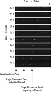
3. After each image is processed as above, a montage of these frames can be created in Graphics Converter X to illustrate the migration of the fluorescent bead as a function of time.

Figure 2: Compiled single frames illustrating bead migration under hydrodynamic flow in the microchannel

White space can used to space and easily identify the specific “snap-shot” images in the compiled file (Figure 2). However, a black fill tool should be applied to this white background to prevent the data being swamped by the background after processing. The image should be exported as an uncompressed JPEG with 8-bit (256 grays) resolution, corresponding to the internal scale required for ImageJ.

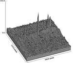
4. The montage JPEG is imported into ImageJ for processing, where the images shown in Figures 1 and 2 are converted to surface plots with the Z axis representing pixel intensity of the image.

Figure 3: Surface plot of data obtained from Figure 1 – illustrating a single frame of the experiment

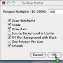
Figure 3 illustrates the surface plot of a single frame, as seen in Figure 1, with Figure 4 illustrating the settings options defined in ImageJ.

Figure 4: Settings menu used in ImageJ to obtain the surface plot functions

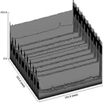
5. The surface plot of the white space corrected Figure 2 can be seen in Figure 5, illustrating the migration over time of a fluorescently labelled microsphere under hydrodynamic flow conditions.

Figure 5: White space-corrected surface plot of Figure 2 data, illustrating the migration over time of a fluorescently labelled microsphere under hydrodynamic flow conditions

It can easily be seen in the figures that data represented in this way significantly improves the quality of the output in terms of usability. It should be noted that the trade-off with this technique is in terms of its limited numerical value due to the conversion and compression across file formats and the subsequent loss of data, especially since one of the major limiting factors is the initial quality and resolution of the images obtained. As such, care should be taken when converting data files and ideally, quantitative data should be extracted from uncompressed files only, so as to maintain integrity.

What else should I know?


Ideally, video files should be recorded using high-speed, high frame rate equipment, thereby facilitating discrimination between events on the microsecond scale, thereby improving resolution and reducing the potential for streaking effects.
However, by careful use of a few relatively easy techniques, low quality AVI movie files (hampered by camera resolution, magnification factors and illumination / contrast issues, all of which are prevalent in microfluidics research), which would not usually stand up as results in a major publication may  be utilised to their fullest potential, and the small white dot of a few pixels in figure 1 representing the fluorescent bead, becomes a distinct peak, easily distinguished from the background signal.
Whilst this work has been conducted using an Apple Macintosh, it should be noted that similar applications are available for computer systems running Windows and Linux. Additionally, the system mentioned is far more versatile than the single application shown in this tip. The range of functions for such low cost software makes this an essential component in the arsenal of any microfluidics researcher.

Digg This
Reddit This
Stumble Now!
Share on Facebook
Bookmark this on Delicious
Share on LinkedIn
Bookmark this on Technorati
Post on Twitter
Google Buzz (aka. Google Reader)

In-line microfluidic bubble trap

David Eddington presents a simple in-line bubble trap for microfluidic devices.

David T. Eddington
Department of Bioengineering, University of Illinois at Chicago, Chicago, IL

Why is this useful?


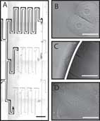
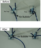
During long-term perfusion of microfluidic channels, bubbles sometimes enter and occlude the channel network as shown in Figure 1A.  In addition, bubbles are cytotoxic to mammalian cells as the surface tension of the air-liquid interface within a microfluidic channel is large enough to rupture cell membranes as shown in Figures 1B-D.  Even when care is taken to fill microfluidic networks and connect tubing without introducing bubbles (see the Tip “Avoiding bubble injection by droplet merging” by Young et al.), bubbles sometimes nucleate within the tubing and enter the channel network causing experiments to fail.  Traditional bubble traps are ineffective for microfluidic systems as these require tubing to connect the bubble trap to the microfluidic device which introduces more opportunities for bubbles to enter the channel network.  To reduce this problem an in-line microfluidic bubble trap has been developed that can be easily integrated into many microfluidic designs.

Figure 1

What do I need?


  • SU-8 mold master
  • PDMS (Sylgard 184, Dow Corning)
  • Razor blade
  • 5mm diameter x 5mm cylindrical spacer (can be adjusted depending on device design)

What do I do?


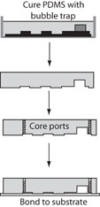
The fabrication of the microfluidic bubble trap is achieved by either molding a well within the network (Figure 2) or by cutting out a well after curing (Figure 3).  If a design is still being iterated, it is easier to cut out the bubble trap after curing.  However, if a final design has been reached, then molding the bubble trap into the network is ideal.  After the bubble trap is cut out or molded, the device is simply bonded to a substrate and when bubbles are introduced into the network they will enter the in-line bubble trap and float to the top as shown in Figure 4.  The volume of the bubble trap can be adjusted depending on the length of the experiments.

Figure 2

Iterated Design (Figure 2)

1. Cure PDMS on master.
2. After peeling the PDMS mold from the master, use the razor blade to cut out a bubble trap. The trap should be deep enough to allow the bubble to rise out of the microchannel.
3. Core access ports through the PDMS mold.
4. Assemble device.

Figure 3

Final Design (Figure 3)

1. Place stainless steel spacers on the master where bubble traps are desired.
2. Pour PDMS over master and cure.
3. After peeling the PDMS mold from the master, remove the steel spacer.  The spacer may need to be cut out of the mold with the razor blade.
4. Core access ports through the PDMS mold.
5. Assemble device.

Figure 4

References


E. W. K. Young, A. R. Wheeler and C. A. Simmons, Avoiding bubble injection by droplet merging, Chips & Tips (Lab on a Chip), 23 October 2006.

Digg This
Reddit This
Stumble Now!
Share on Facebook
Bookmark this on Delicious
Share on LinkedIn
Bookmark this on Technorati
Post on Twitter
Google Buzz (aka. Google Reader)

A simple interface between a PDMS microfluidic device and a syringe

Jeonggi Seo and Meng H. Lean present a simple way to connect a syringe to your microfluidic device without the need for adhesive.

Jeonggi Seo and Meng H. Lean
Palo Alto Research Center, Palo Alto, CA, USA

Why is this useful?


Syringes are commonly used to supply or collect liquid samples for microfluidics. However, interfacing between a microfluidic chip and syringe is problematic due to their size difference. Plastic tube connectors or Luer stubs have been used as interfacing methods, but they increase sample dead volume and thus experimental cost. The goal of this tip is to provide an inexpensive and simple interface, with minimized sample dead volume, between a microfluidic device and syringe.

Figure 1.

What do I need?


  • 18 gauge blunt needle
  • PTFE microbore tubing (0.012″ID x 0.030″OD, Cole Parmer)
  • Silicone (platinum-cured) tubing (1/50″ID x 1/12″OD, Cole Parmer)
  • B-D Disposable Syringes 1 mL

What do I do?


1.Punch access holes into your PDMS device with an 18 gauge blunt needle.

2.Cut a segment of silicone tubing ~10 mm long. (Figure 1)

3.Cut a segment of PTFE microbore tubing with desirable length for your set-up.

Figure 2.

4.Insert the piece of silicone tubing inside the 1 ml syringe tip. Make sure the silicone tubing reaches the inner chamber of the syringe but doesn’t disturb piston movement. (Figure 2a-c)

5.Insert the PTFE tubing into the inserted silicone tubing. (Figure 2d)


Figure 3.

6. Load your sample into the syringe

7. Insert the free end of the PTFE tubing into the access hole on your PDMS device (Figure 3). Since no adhesive is involved, the PTFE tubing can be disposed of or reused after cleaning.

References


S. Mohanty, G. Mensing and D. J. Beebe, PDMS connectors for macro to microfluidic interfacing, Chips & Tips (Lab on a Chip), 23 October 2006.

Digg This
Reddit This
Stumble Now!
Share on Facebook
Bookmark this on Delicious
Share on LinkedIn
Bookmark this on Technorati
Post on Twitter
Google Buzz (aka. Google Reader)