Archive for the ‘Fabrication’ Category

Integrated reservoirs for PDMS microfluidic chips

T. Liu, E. V. Moiseeva, and C. K. Harnett
Electrical and Computer Engineering, University of Louisville, Louisville, KY 40208, USA

Purpose


Reservoirs are sometimes preferable to tubing connections, especially for pressurized or gravity-driven flow, for installing electrode wires into open ports, or for storing a PDMS chip pre-loaded with water to preserve its hydrophilicity after plasma treatment. However, gluing individual reservoirs onto a finished chip can be messy and prone to clogging ports and channels with silicone, and the assembly may be fragile. These reservoirs, made from inexpensive nylon spacers, are embedded in the chip by PDMS casting, eliminating several of these problems. They can run with up to 30 psi gas pressure-driven flow when provided with connections for pressurized tubing.

Materials


Consumables:

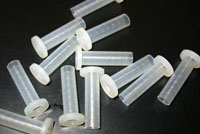
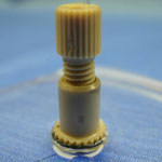
  • Flanged nylon shoulder spacers (McMaster Carr part 91145A154, shown in Figure 1)
  • PDMS compound (Dow Corning Sylgard 182 or 184)

Figure 1: Flanged nylon shoulder spacers for use as reservoirs

For optional gas pressure-driven flow:

  • Epoxy (Scotch-Weld DP-420)
  • Hose barb connectors (McMasterCarr part 51525K211)

Tools:

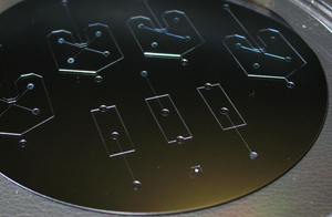
  • A mold for casting chips (Figure 2)
  • PDMS weighing and degassing equipment
  • A punching tool for creating ports in PDMS, such as thin-walled stainless hypodermic Tubing (Small Parts Inc., part HTX-22X or similar)
  • Tweezers
  • X-Acto knife

Figure 2: A microfabricated mold on a 4-inch silicon wafer

Procedure


1. Make a mold for your design, with reservoir locations 1 cm apart or more. This method was tested on SU-8 molds on silicon wafers, with resist thickness from 60 to 170 microns, without any special mold release treatment.

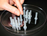
Pour a thin (~1 mm) layer of PDMS over the mold, and cure until solid. Place the nylon standoffs on top of the PDMS layer, over the ends of your channels, flange side down. Later you will punch to connect the reservoir with the channel on the underside of the chip. These reservoirs easily stay upright if the PDMS is still a bit sticky. (Figure 3)

Figure 3: Reservoirs are placed on a thin layer of PDMS cured over the mold

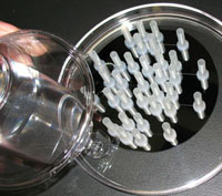
Figure 4: A second layer of PDMS holds the reservoirs in place

2. Pour a second 2 mm or thicker layer of PDMS around the reservoirs, covering the flanges to anchor them. (Figure 4) It doesn’t matter if PDMS seeps into some of the reservoirs. Let the PDMS level out, then cure until solid. The nylon reservoirs are OK at temperatures up to 80ºC.

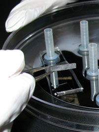
3. Cut out individual devices with the X-Acto knife and peel off devices plus embedded reservoirs. It’s best to grip the devices at the PDMS using tweezers, rather than pulling on the reservoirs. (Figure 5)

Figure 5: Reservoirs and channels are removed from the mold together

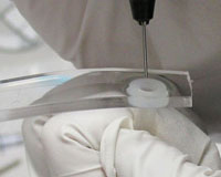
4. Use the punching tool to create a port in each reservoir that connects to the microfluidic channel, making sure to remove a core of PDMS from each port. This can be done from the channel side (Figure 6) or from the reservoir side.

Figure 6: Punched ports connect reservoirs to channels

5. Bond the punched chips to a glass, PDMS or other substrate using plasma activation or other method of choice. Figure 7 is a side view of a bonded chip, showing anchored reservoirs and punched ports on a molded PDMS chip, attached to a blank PDMS slab on a glass slide.

Figure 7: Side view of a sealed chip showing sunken reservoirs and ports

6. (Optional, for gas pressure-driven flow) Use epoxy to attach hose-barb connectors to the tops of any reservoirs you want to pressurize. Gas can be provided to each reservoir using Tygon tubing. The 1/16″ hose barb to Luer connectors, and 1/16″ ID Tygon tubing are a good match to the size of these reservoirs. Gluing adjacent Luer connectors together can help strengthen the assembly when several gas connections are anticipated.

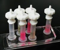
7. Fill reservoirs through the open tops or through the bonded-on hose barbs. Dispensing from a syringe with a long needle or a needle threaded into a small diameter piece of tubing helps prevent trapped air by filling from the bottom up. Figure 8 shows a filled chip with barbs for gas tubes.

8. While these reservoirs have been pressurized up to 30 psi before delaminating, they are easily removed from the chip by bending them sideways. Reservoirs can be peeled out of old chips for re-use if needed.

Figure 8: A filled chip ready for gas pressure-driven flow
Digg This
Reddit This
Stumble Now!
Share on Facebook
Bookmark this on Delicious
Share on LinkedIn
Bookmark this on Technorati
Post on Twitter
Google Buzz (aka. Google Reader)

Microfabrication design guidelines for glass micro- and nano-fluidic devices

Dave Hubera and Sumita Pennathurb
a Stanford Genome Technology Center, Stanford University, Stanford, CA, USA
b Department of Mechanical Engineering, University of California, Santa Barbara, CA, USA

Why is this useful?


Lab on a Chip devices fabricated with silicon dioxide or glass substrates represent the gold standard for many applications due to their robustness and repeatability.  However, fabricating these devices can be time consuming and expensive, particularly compared with devices created using rapid prototyping methods such as PDMS molding.  Therefore, in this edition of “chips and tips” we highlight a few of the issues that arise when designing and microfabricating fluidic devices and suggest tips that, we hope, will save you time, money, and perhaps another trip to the clean room.

1. Finding yourself – registration marks


Identifying a location in a channel with high precision can be very difficult, particularly when you are observing long stretches of otherwise featureless channels through high magnification objectives.  While this can be accomplished with expensive, high-resolution, motorized stages, it can also be accomplished elegantly using on-chip registration marks, such as rulers or other indicators.  Registration marks can be designed and fabricated with very little additional effort, by adding them to your channel mask design and subsequently etching the marks and fluidic channels in the same step.  But beware; if registration marks are too close to channels, minor lithography and etching errors can result in a poor seal and lead to leaks.  Recall that isotropic etching will produce channel (and mark) widths larger than the dimensions in the mask, so it is necessary to account for the final widths when positioning your marks relative to the channels.
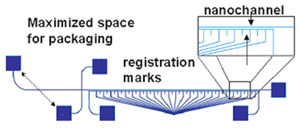
Figure 1: Schematic of a nanofluidic separation device with the following design considerations: 1) maximized space for packaging between the inlet holes, 2) on chip filters at the inlets, and 3) registration marks below the separation channel. In this particular design the registration marks are a separate, contiguous channel that can be filled with dye to aid in locating the adjacent separation channel (see Tip 5).

Ultimately, the selection of mark location relative to the channel is application dependent.  For greatest convenience, the marks and channels should appear within the same field of view on your microscope.  However, if your detection signal is very low, the presence of the marks may introduce additional noise (see tip 5).  In this case, it is preferable to locate your registration marks outside the field of view containing the channels.  Figure 1 shows a cross-channel design that includes tick marks underneath the separation channel.

2. Keeping it clean – on chip filters


All microfluidic chips eventually accumulate debris within the channel that can compromise performance or, worse, block the channel entirely.  Incorporating filters into your channel can help extend the working life of your devices.  These on-chip filters can be structures like pillars and, like registration marks, can be included in a design with little or no extra fabrication costs.  However, the design of the filter regions is critical if they are to successfully protect your channels without introducing other problems.  For example, when significant dead volumes are present, it becomes difficult and time-consuming to exchange samples or buffers because you must rely on diffusion to clear previous solutes from the dead volumes.  Figure 2 shows leakage of a fluorescent analyte from dead volumes at the corners of a square filter pad.  Here are some design considerations for on-chip filters:

  • Dead volumes arise when areas are not effectively flushed by fluid flow through the device. The filter shape should ensure that all regions experience approximately the same magnitude of fluid flow.  Also, sharp corners should be avoided. If necessary, lengths should be minimized to decrease the distance over which analytes must diffuse to escape the corner’s dead volume.
  • Large particles are excluded from the channel by the filter elements.  Consequently, filter elements should be sized to exclude the greatest number of particles.  However, the spacing between the elements should not be significantly smaller than the dimensions of the main channels or they can influence the behavior of the device.  For example, a spacing below 1 µm can result in concentration polarization effects due to the influence of the electric double layer.[1]
  • Small particles are trapped via adsorption to filter walls.  Trapping efficiency increases with the residence time of particles within the filter.  Thus, the filter area should be large relative to that of the channel.
  • The positioning of via holes may vary significantly, particularly if alignment of the channel and lid wafers is performed by eye (with no alignment tool) prior to bonding.  The design should allow for variation in the mating of the lid and the channel wafer, to ensure that filters are not bypassed by slightly misaligned via holes.

A simple on-chip filter schematic that minimizes dead volume is shown in Figure 2(b).  Many other designs are possible, and tradeoffs may be made between flow uniformity and areal expansion at the entrance to the filter.  Note, also, that filter designs can vary based on the design of the vias.
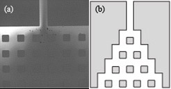
Figure 2: (a) Square on-chip filter design showing leakage of fluorescent dye from the corners of the filter. The dark region in the center indicates the region effectively flushed by fluid flow. In such designs, buffer or analyte exchange is extremely difficult due to dead volume in the corners. (b) A sample design that minimizes dead volume.

3. It’s not just the inside, the outside counts – fluidic interconnects


Many researchers have difficulty interfacing their microfluidic device with off-chip tubing, syringes, etc.  In a previous edition of Chips and Tips, the authors described a quick and cheap syringe tubing interface.[2]  Other solutions include commercially available options such as Labsmith[3] and Upchurch[4] fittings.  However, whichever interface you select, you must remember to allocate sufficient space for the connections on your device.  In general, these connectors are orders of magnitude larger than channel widths, and it is not uncommon to have channel lengths about the size of a fitting.  If a channel is too short, the fittings will overlap.  Even if they fit on the chip, the fittings may be so close as to interfere with their operation (e.g., loosening and tightening, adding or removing tubing) or with device function (e.g., introducing reflected light or autofluorescence into the detection region).  If the channel length must be on the order of the fitting size, we recommend that you design the ports such that you can maximize the space between them, for an example, see Figure 1.  Finally, be aware that the change in volume between the interconnect and the inlet of the microfluidic device may induce flow effects, such an nonlinear electrokinetic instabilities in the case of electroosmotic flow, and geometry induced vortices at sharp corners[5] – so be careful to design the channel to be long enough to neglect these (mostly harmful) hard-to-predict entrance effects in the main part of the channel.

4. Getting it together – bonding


Poor bonding between a channel wafer and its cover plate is a common cause of device failure.  It is particularly frustrating because bonding is the last significant fabrication step, after many hours have already been invested.  Many different bonding techniques (e.g., sacrificial bonding layers[6], spin-on glass[7-8], low temperature annealing with NaOH[9], and adhesive bonding[10]) have been developed; however, fusion bonding remains the most robust and reliable option for glass devices that can withstand the high temperatures required.  Therefore, we present a recipe (including a few tricks) to help achieve reliable fusion bonds between glass substrates:

  1. Before processing, ensure your substrates are sufficiently flat.  Inexpensive commercial glass wafers are often not flat enough to achieve a fusion bond.  If this is your only option, however, we recommend that you lap and polish the wafers prior to any processing.  Both the top and bottom substrate of the microfluidic chip must be lapped and polished.
  2. Clean and process your wafers.  Avoid processes that will roughen the bonding surface on the wafer because this reduces the surface area available for bonding and may lead to weakened substrates.
  3. After processing, thoroughly clean both top and bottom substrates using the following recipe.  Particulates or films will interfere with bonding. 20 minute clean in H2SO4 (90%) + H2O2 (10%) at 115º, 10 minute rinse with deionized (DI) water, spin rinse and dry (or dry very carefully by hand with clean nitrogen) .
  4. Hydrolyze the channel and cover wafers with a standard RCA1 clean, listed below, in order for the wafers to be completely clean and particulate free for the mating step. 10 minute clean in H2O (70%) + H2O2 (15%) + NH4OH (15%) at 80ºC, 10 minute rinse in DI water, spin rinse and dry (or dry very carefully by hand).
  5. Remove the native oxide that has formed on the wafers during processing with a short HF dip.  The etch should be sufficiently short to remove the oxide without etching the underlying channels. 20 second dip in 50:1 HF, 10 minute rinse with DI water, spin wash and dry (or dry very carefully by hand).
  6. Once the wafers are dry, position the channel wafer over the cover wafer such that your features align, then press the wafers together.  In a successful bond, you will see a wave of fringe patterns progress across the wafer, as the Van der Waals forces cause the wafer to pre-bond.  (It may be helpful to lightly bow one wafer by pressing on the center of one wafer, then releasing the wafer edge once contact is made in the center.)  These fringe patterns (or Newton rings) indicate the topology at the interface of the wafers and are only visible when the wafers are in intimate contact.  Particles will be surrounded by fringes (the number of fringes indicating the height of the particle).  In a perfect bond, all fringes will appear at the edge of the wafer.  If many particulates or fringes appear across the wafer, the bond will likely be poor, so separate the wafers and repeat steps 1-5.
  7. Place pre-bonded wafers in an oven (no vacuum needed, no weight needed) for 4-5 hours at the softening temperature of the material (500-600ºC for borofloat glass, 1100-1200ºC for quartz and fused silica).  We recommend ramping the temperature to the softening temperature, so as not to induce thermal stresses within the material.

5.  You’re special – special considerations for nanochannels


Nanochannels offer interesting new opportunities for studying nanoscale physics and performing fluidic operations on a scale less than that of a single cell; however, their size and the interfacial effects associated with their large (relative) surface areas introduce additional concerns.  Channel filling is a significant one and is generally accomplished via capillary action.  To do so, avoid introducing hydrophobic regions at the entrance of your channel (e.g., gold electrodes) and ensure your channels are not too long.  Of course, “too long” is dependent on your channel dimensions, for example, a 100 nm tall nanochannel longer than 50 cm will not fill successfully via wicking alone.  For long channels or adverse wicking conditions, you will need to apply pressure-driven flow.  The challenge with nanochannels is that their hydraulic resistance is large and high pressures are required to generate appreciable Poiseuille flow.  These pressures can easily be larger than those generated by syringe pumps (over 200 psi) and require high pressure fittings and interconnects.  Pressure filling in nanochannels can also introduce bubbles in the channel which are almost impossible to remove.

In nanoscale devices it can be challenging to locate the channels.  When channels are sufficiently wide, they can usually be seen under brightfield imaging, when channels are narrow (< 1µm) or nanofluidic chips are used for fluorescence measurements (i.e., in the dark), it is extremely difficult to find them, and the use of registration marks (see Tip 1) is critical.  When using registration marks with nanochannels, we recommend connecting the marks together into a parallel channel system with its own inlet and outlet.  The marks can be then be filled with fluorescent dye.  In this way, you can both locate the channel and also use the fluorescence intensity of the marks as a reference. However, keep in mind that the fluorescence from the channel may overwhelm the signal of a low concentration or dim analyte, so you may want to design the marks to be located just outside of the channel field of view.

References


[1] F. C. Leinweber, U. Tallarek, Langmuir, 2004, 20, 11637-11648.
[2] R.Martinez-Duarte and M. Madou, Quick and cheap syringe-tubing interfacing, Chips & Tips (Lab on a Chip), 26 June 2007.
[3] http://www.labsmith.com
[4] http://www.upchurch.com; A. Persat, T. Zangle, J. Posner and J. Santiago, On-chip electrophoresis devices: do’s, don’ts and dooms, Chips & Tips (Lab on a Chip), 26 March 2007.
[5] A. P. Sudarsan, V. M. Ugaz, Proc. Natl. Acad. Sci. U.S.A., 2006, 103, 7228-7233.
[6] A. Sayah, D. Solignac, T. Cueni and M. A. M. Gijs, Sens. Actuators, A, 2000, 84, 103-108.
[7] A. Satoh, Sens. Actuators, A, 1999, 72, 160.
[8] R. Puers amd  A. Cozma,  J. Micromech. Microeng., 1997, 7, 114.
[9] S. C. Jacobson, A. W. Moore, and J. Ramsey, Anal. Chem., 1995, 67 , 2059.
[10] Y. J. Pan and R. J. Yang, J. Micromech. Microeng., 2006, 16, 2666-2672.

Digg This
Reddit This
Stumble Now!
Share on Facebook
Bookmark this on Delicious
Share on LinkedIn
Bookmark this on Technorati
Post on Twitter
Google Buzz (aka. Google Reader)

Bonding Upchurch® NanoPorts to PDMS

Corey Koch, James Ingle, and Vincent Remcho
Department of Chemistry, Oregon State University, Corvallis, Oregon, USA

Why is this useful?


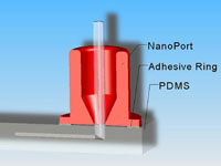
Upchurch (Oak Harbor, WA, USA) NanoPorts are one of the few commercial products on the market for making chip-to-world connections. NanoPorts are robust, easy to use, able to connect to standard tubing sizes (1/16-in OD and capillary tubing), and are particularly useful when connections are changed regularly. These fittings are constructed from polyetheretherketone (PEEK) and are intended to adhere to glass or silicon surfaces using epoxy or a heat-curable adhesive ring. The adhesive ring is compatible with many types of materials and NanoPorts have been used on a variety of polymers such as polycarbonate, cycloolefin (Zeonor), polyimide (Kapton), and polymethylmethacrylate.1-4 Unfortunately, NanoPorts do not readily adhere to one of the most common materials for prototyping microfluidic devices, polydimethylsiloxane (PDMS), and NanoPorts are often bonded to another material (commonly glass) in PDMS hybrid devices.5 A useful tip from Upchurch technical support is to imbed the NanoPorts into the PDMS chip during curing, but this can be cumbersome and PDMS only conformally seals to the PEEK surface so leakage can easily occur at the PDMS-PEEK interface. Fortunately, a tool common to the PDMS fab-lab, the oxygen plasma, can be used to bond PDMS to other substrates with the adhesive rings Upchurch supplies. Using an oxygen plasma to bond PDMS chips together using an adhesive tape has been mentioned in the literature,6 and this tip expands upon that work to form bonds between NanoPorts and PDMS using the supplied adhesive rings after exposing the PDMS surface to an oxygen plasma. It should be noted that the majority of this work was performed with the now unavailable acrylic-epoxy hybrid rings (3M Surface Bonding Tape 583), but the tip also works well with the new MEG-150 polyamide-epoxy resin adhesive ring.

What do I need?


  • Fully cured PDMS (Dow Corning Sylgard 184) microchip with via holes to microchannels
  • Upchurch NanoPort and supplied adhesive ring
  • Oxygen plasma or another source to oxidize the PDMS surface (simple methods based on corona discharge, peroxide, and a home-microwave have been presented in the literature)7,8,9
  • Clamp (try aluminum plates and a C-clamp or cantilever clamp)
  • A heat source (convection oven recommended)

What do I do?


1.  Prepare the PMDS microchip and NanoPort for bonding (Figure 1). Ensure the surfaces are fresh or clean with alcohol and air dry. If you are using the acrylic-epoxy hybrid adhesive ring, remove one side of the backing and stick it to the bottom of the NanoPort.

Figure 1.

2.  Oxidize the PDMS surface. This is commonly done in an oxygen plasma (Figure 2). Conditions vary, but based on experience and literature studies10,11 a pressure of 100 mTorr (oxygen gas), 20 W of RF power, and a 30 s exposure time provide an appropriate surface for bonding (ensure the surface is exposed to the plasma as in Figure 2).

Figure 2.

3. Quickly remove the PDMS from the plasma chamber and place the NanoPort with adhesive ring over the via hole to your microchannel (Figure 3). If you are using the new polyamide-epoxy resin adhesive ring, it is easier to place it on the oxidized PDMS surface using tweezers (because it is not tacky and won’t stick to the NanoPort bottom) and then set the NanoPort on top of it.

Figure 3.

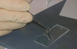
4.  Clamp the NanoPort-adhesive-PDMS assembly and place it in an oven for the recommended curing time and temperature (see Upchurch technical notes and adhesive links, conditions vary based on the adhesives and temperatures used). For the acrylic-epoxy adhesive ring, a curing time of 2.5 hr at 100°C was used; for the polyamide-epoxy resin adhesive ring, a cure time of 1.5 hr at 165°C was used. Polycarbonate blocks (Figure 4) can be used for clamping at lower temperatures (< ~140°C); aluminum is suggested for higher temperatures.

Figure 4.

5. Your well-bonded NanoPort interconnect to PDMS is now ready to use! (Figures 5 and 6). In control experiments without plasma exposure, neither adhesive adhered to the PDMS and they fell off with minor stress. Testing the bond directly after contacting the ring to oxygen plasma-activated PDMS surface (before heat cure) demonstrates bonding to the PMDS surface but not to the PEEK NanoPort. Failure testing of a completely bonded NanoPort results in tearing of the PDMS with the ripped polymer remaining on the adhesive ring. Bonds formed with the acrylic epoxy hybrid ring consistently withstood pressures up to 24 psi and several bonds withstood pressures above 40 psi, making the interconnect robust at pressures in the range of PDMS material failure (30-50 psi).12

Figure 5.

Figure 6.

Acknowledgements


This material is based upon work supported by the National Science Foundation under Grant No. DGE-0549503. This research was also supported by a research grant from the U.S. Environmental Protection Agency sponsored Western Region Hazardous Substance Research Center under agreement R-828772. This work has not been reviewed by the agency, and no official endorsement should be inferred.
References


[1] A. Muck and A. Svato, Rapid Commun. Mass Spectrom., 2004, 18, 1459-1464.
[2] S. J. Hart, A. Terray, T. A. Leski, J. Arnold and R. Stroud, Anal. Chem., 2006, 78, 3221-3225.
[3] Y. Yang, J. Kameoka, T. Wachs, J. D. Henion and H. G. Craighead, Anal. Chem., 2004, 76, 2568-2574.
[4] R. Barrett, M. Faucon, J. Lopez, G. Cristobal, F. Destremaut, A. Dodge, P. Guillot, P. Laval, C. Masselon and J.-B. Salmon, Lab Chip, 2006, 6, 494-499.
[5] L. A. Legendre, J. M. Bienvenue, M. G. Roper, J. P. Ferrance and J. P. Landers, Anal. Chem., 2006, 78, 1444-1451.
[6] L. Xie, S. C. Chong, C. S. Premachandran, D. Pinjala and M. K. Iyer, Electronics Packaging Technology Conference, 2005, 93-97.
[7] K. Haubert, T. Drier and D. Beebe, Lab Chip, 2006, 6, 1548-1549.
[8] G. Sui, J. Wang, C. C. Lee, W. Lu, S. P. Lee, J. V. Leyton, A. M. Wu and H. R. Tseng, Anal. Chem., 2006, 78, 5543-5551.
[9] B. T. Ginn and O. Steinbock, Langmuir, 2003, 19, 8117-8118.
[10] S. Bhattacharya, A. Datta, J. M. Berg and S. Gangopadhyay, J. Microelectromech. Syst., 2005, 14, 590-597.
[11] B.-H. Jo, L. M. Van Lerberghe, K. M. Motsegood and D. J. Beebe, J. Microelectromech. Syst., 2000, 9, 76-81.
[12] J. C. McDonald, D. C. Duffy, J. R. Anderson, D. T. Chiu, H. Wu, O. J. A. Schueller and G. M. Whitesides, Electrophoresis, 2000, 21, 27-40.

Digg This
Reddit This
Stumble Now!
Share on Facebook
Bookmark this on Delicious
Share on LinkedIn
Bookmark this on Technorati
Post on Twitter
Google Buzz (aka. Google Reader)

Magnets for facile molding of via holes in PDMS

Corey Koch, James Ingle, and Vincent Remcho
Department of Chemistry, Oregon State University, Corvallis, Oregon, USA

Why is this useful?


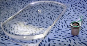
The formation of vias between microchannels in PDMS and fluidic interconnects is commonly performed by using a punch to cut away PDMS. This process often results in a torn surface that is not as resilient to pressure driven flow, can create material that clogs channels, provides less control of hole shape, and results in the formation of irregular surfaces that increase dead volume.[1] A smoother surface finish and more controllable hole geometries have been achieved by using posts in the molding process.[2] Magnetic fixturing of via holes provides a readily configurable and facile means to locate and hold posts. Magnets also come in all shapes and sizes and can therefore provide a creative means to incorporate mesoscale features into PDMS microchips. In this example, cylindrical neodymium magnets are used to mold via holes into a PDMS microchip.

What do I need?


  • Magnets for molding. Neodymium magnets provide the strongest field and are available commercially in a variety of shapes and sizes.
  • A microchip master mold. Guide features on the microchip master can aid magnet alignment.
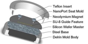
  • A PDMS molding fixture that can attract magnets. A mold made from a ferromagnetic material (such as steel) or placing a magnetic base below a plastic or aluminum fixture, as shown in Figure 1, can provide a means to hold the magnets.
  • PDMS (Dow Corning Sylgard 184).
  • In this example, a flat surface was necessary above the via hole to bond Upchurch NanoPorts as interconnects. Because PDMS forms a meniscus on the surface around the magnet when curing, a steel cylinder was placed above the via hole molding magnet to create a NanoPort mating seat.
    Figure 1

What do I do?


1.  Prepare your master mold, magnetic PDMS mold (An SU-8 on silicon microchip master mold and steel base are shown as an example in Figure 2), and your magnets.

Figure 2

2.  Place the magnets on the appropriate guide features on the master mold as shown in Figure 3. In this example 1/8″ high by 1/16″ diameter cylindrical magnets and a specially designed plastic mold with a steel base (as shown in Figure 1) were used. An aluminum foil mold as described in “Chips and Tips: Rapid curing of PDMS for microfluidic applications” could be used for a quick and easy molding platform.
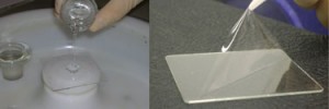
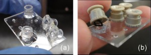
Figure 3

3.  In this example a flat surface is needed for bonding Upchurch NanoPorts, so a steel cylinder (Figure 4) with a diameter greater than the NanoPort is placed on top of the magnet to move the PDMS meniscus away from the center of the via hole and provide a flat seat for bonding.

Figure 4

4.  Pour the PDMS as shown in Figure 5 (mixed to manufacturer specifications or for your specialty application). Bubbles can get trapped under the steel ‘NanoPort seat’ so fill the mold slowly or degas after filling.

Figure 5

5.  Cure the PDMS at your desired temperature. Remove the PDMS from the mold and use a tweezers to pull out the magnet. Cut the chip to size as shown in Figure 6 and notice the quality of your now ready via hole!

Figure 6

6.  In this example, the steel ‘NanoPort seat’ provided a flat surface to bond the NanoPort, and the meniscus actually allows for rapid registration of the NanoPort to the via hole (Figure 7). The 1/8″ high by 1/16″ diameter magnets used can be placed close enough for maximum NanoPort packing density (magnets within 5 mm of each other).

Figure 7

Using magnetic posts can provide a variety of shapes and sizes of via holes, a smooth hole, and a convenient method for securing posts during molding.

Another quick tip for using 1/16″ tubing: employ 1/16″ diameter cylindrical magnets and tubing with a small ID. Cut the tubing at a slight angle and insert it to the bottom of the via hole to minimize dead volumes in your interconnect.

Acknowledgements


This material is based upon work supported by the National Science Foundation under Grant No. DGE-0549503. This research was also supported by a research grant from the U.S. Environmental Protection Agency sponsored Western Region Hazardous Substance Research Center under agreement R-828772. This work has not been reviewed by the agency, and no official endorsement should be inferred. We would like to recognize Ted Hinke at the Oregon State University Department of Chemistry Machine shop for his help in mold design and his skill in its construction.

References


1] S. Li and S. Chen, IEEE Transactions on Advanced Packaging200326, 242-247.
[2] D. C. Duffy, J. C. McDonald, O. J. A. Schueller and G. M. Whitesides, Anal. Chem.199870, 4974-4984.

Digg This
Reddit This
Stumble Now!
Share on Facebook
Bookmark this on Delicious
Share on LinkedIn
Bookmark this on Technorati
Post on Twitter
Google Buzz (aka. Google Reader)

A foolproof method for enclosing glass-based LOC devices for electrophoresis

Colin D. Mansfield, Radoslaw Mazurczyk and Julien Vieillard
Institut des Nanotechnologies de Lyon, Ecole Centrale de Lyon, France

Why is this useful?


Bonding of glass-based lab-on-a-chip (LOC) devices presents a challenging, time-consuming problem, often requiring specialist equipment and skills. Moreover, it is fraught with dangers that if the typically elaborate protocol [1-3] is not strictly followed, then the chip’s channels may leak, ruining an otherwise perfectly good device. Ironically, successful bonding can also be a liability, a chip’s lifetime being reduced due to the difficulties and ambiguity associated with thoroughly cleaning its channels between experiments. Other factors that make bonding of glass-based microdevices problematic include: (i) the inherent nanometre roughness of glass (which renders direct glass-glass bonding a non-trivial task); (ii) low-temperature requirements imposed by possible integration of opto-electronic components; (iii) certain processes, (e.g. ion-exchange waveguide integration) can introduce surface defects (~200 nm in height) that preclude any possibility of glass-to-glass bonding without planarization.

This tip describes a simple, inexpensive and reversible solution to enclose microchannels, using a sheet of polydimethylsiloxane (PDMS). It avoids all the pitfalls mentioned; the natural compliance and adhesion of the PDMS sheet conforms efficiently to the glass substrate’s topography to form a leak-free seal, while the ‘bonding’ is performed at room temperature with very basic equipment. Moreover, since the PDMS layer is easily peeled away from the substrate, there are no consequences if the initial alignment fails and there is full access to the microchannels during cleaning, allowing chips to be recycled.

What do I need?


  • Sylgard 184 silicone elastomer kit (DowCorning).
  • Flat glass support, preferably with raised edges.
  • Measuring cylinder, beaker, plastic stirrer, xylene, paper towels.
  • Cutter, ruler, print-off of device geometry, hole punch, tweezers.
  • Oven, spin-coater (optional).Mix PDMS and curing agent in a 10:1 weight ratio in a disposable weigh boat.

What do I do?


1.  PDMS is messy stuff, so first cover the working area with paper towels to catch any spills.

2.  Mix the base polymer and curing agent in a ratio of 10:1 and stir vigorously for 5 minutes to obtain a homogeneous solution. (For a 15 x 15 cm glass support, approximately 16.5 ml and 55 ml total volume produces sheets of thickness 0.75 mm and 2.5 mm respectively).

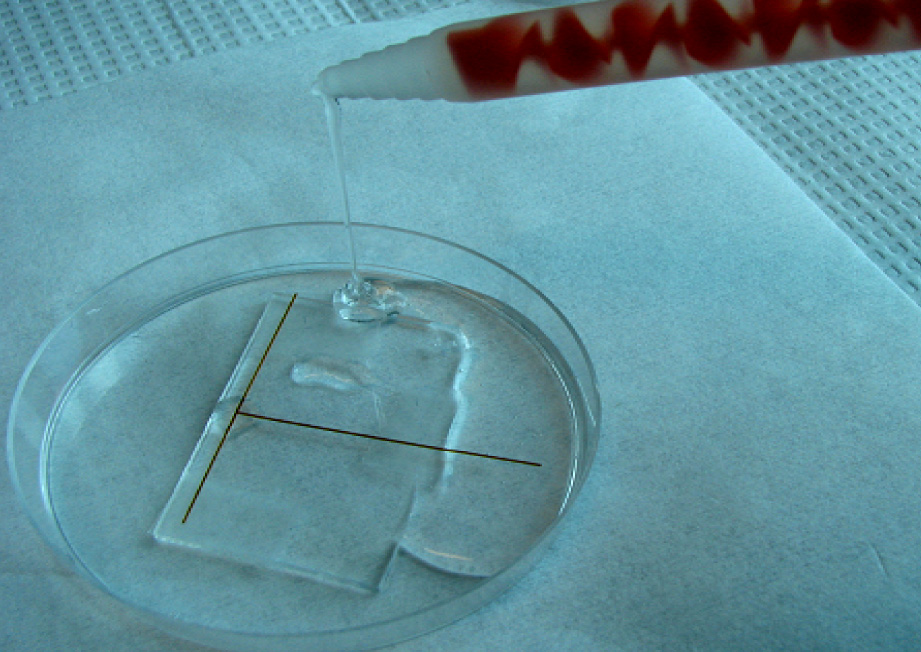
3.Pour this mixture evenly onto the glass support and let it rest for 1 hour to degas and flow (Figure 1). (This process can be accelerated by placing it into a ultrasonic bath for 5 min before pouring).

Figure 1. Degassed PDMS mixture being poured onto glass support.

4.  Place the glass support onto a flat surface in the oven and bake for 1 hour at 100 °C. (Alternatively, 24 hours at room temperature or 30 min at 120°C also work well).

5.  Once cooled, place the glass support over your template and scribe around the LOC’s perimeter. If access ports are required, use the punch (e.g. 2 mm outer diameter) to cut out  holes, taking care not to leave any shreds (Figure 2).

Figure 2. PDMS being shaped to LOC geometry.

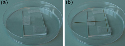
6.  Remove the PDMS cover with plastic tweezers and place it over your prepared LOC (Figure 3), ensuring that the side in contact with the support’s surface is face-down. Any trapped air is easily expelled by applying light pressure to the PDMS and pushing it towards the edge. If you are unhappy with the final alignment or cannot remove some trapped air, simply peel off the PDMS layer and repeat this step.

Figure 3. Application of PDMS cover to glass LOC.

7.  For clean-up of PDMS pre-polymer liquid, we have found the solvent xylene works well.

What else should I know?


Since it is simple to control the thickness of the PDMS sheet it is also possible to fabricate ‘windows’ of < 50 µm thickness, thereby enclosing the channel and also allowing a delivery/collection fibre to be positioned in very close proximity to the microchannel [4]. The protocol is as described above, however, there is no need for degassing and the layer is prepared using a spin-coating method (1500 rpm, 40 s) onto a glass slide (6 x 6 cm) (Figure 4).

Figure 4. Spin coating of a thin (< 50 µm) PDMS sheet.

Based upon a PDMS cover of 75 x 25 x 0.75 mm, we estimate the cost of this method to be less than 15 pence/device. This may be especially beneficial to teaching establishments that can use a small number of glass etched devices many times over for practical courses. Although this approach has proven viable in electrophoretic studies,[4] it does have some limitations. Namely, (i) plug flow will be distorted at the glass/PDMS interface, deteriorating separation performance and (ii) proteins are prone to adsorption by the PDMS, worsening the resolution of electrophoresis and hindering the detection of trace proteins. The good news is however, that if data acquired using such a hybrid device shows any signs of promise, your efforts in fabricating a fully glass-bonded chip are certain to be rewarded.

Acknowledgements


Colin Mansfield acknowledges the financial support of the European Community under a Marie Curie Intra-European Fellowship, administered by Dr S Krawczyk.

References


[1] A. Iles, A. Oki and N. Pamme, Bonding of soda-lime glass microchips at low temperature. Microfluid. Nanofluid., 2007, 3, 119-122.
[2] L. Chen, G. Luo, K. Liu, J. Ma, B. Yao, Y. Yan and Y. Wang, Bonding of glass-based microfluidic chips at low- or room-temperature in routine laboratory, Sens. Actuators, B, 2006, 119, 335-344.
[3] N. Chiem, L. Lockyear-Shultz, P. Andersson, C. Skinner and D. Jed Harrison, Room temperature bonding of micromachined glass devices for capillary electrophoresis. Sens. Actuators, B, 2000, 63, 147-152.
[4] R. Mazurczyk, J. Vieillard, A. Bouchard, B. Hannes, S. Krawczyk, A novel concept of the integrated fluorescence detection system and its application in a lab-on-a-chip microdevice. Sens. Actuators B, 2006, 118, 11-19.

Digg This
Reddit This
Stumble Now!
Share on Facebook
Bookmark this on Delicious
Share on LinkedIn
Bookmark this on Technorati
Post on Twitter
Google Buzz (aka. Google Reader)

Organic solvent compatible reservoirs for glass microfluidic chips

Michael W. L. Watson and Aaron R. Wheeler
Department of Chemistry, University of Toronto, Ontario, Canada

Why is this useful?


Some applications for microfluidics, such as synthesis, reversed phase separations, and liquid-liquid extraction, require the use of organic solvents (e.g. acetonitrile, methanol, etc.).  For such applications, glass or quartz substrates are preferred; however, even when using solvent-resistant substrates, such applications are often limited by the problem of connecting reservoirs to the substrate. As illustrated in Figure 1, common adhesives used for this purpose, such as epoxies and UV cured glues, are not able to withstand extended periods of exposure to solutions with high organic solvent content.

Figure 1: Reservoirs connected with traditional adhesives

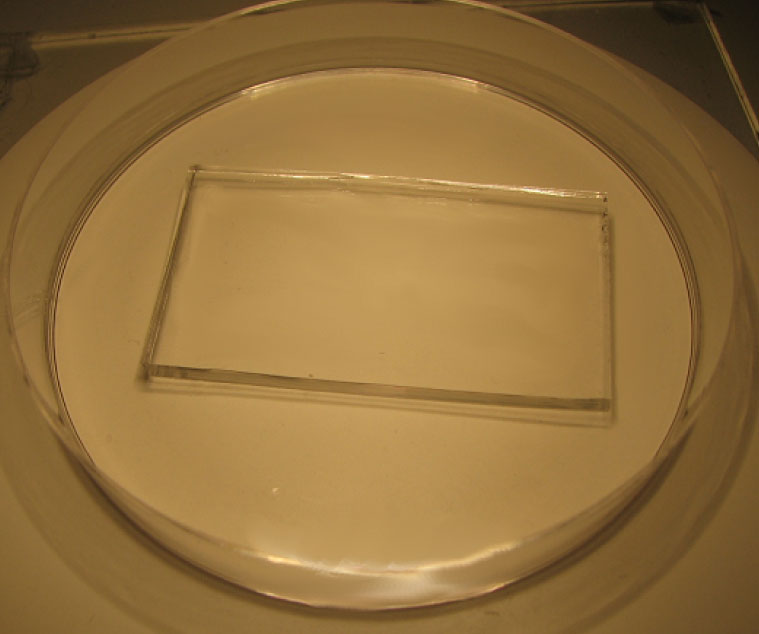
In this Tip, we report a straightforward solution to this problem: using an oxygen plasma bonded poly(dimethyl siloxane) (PDMS) reservoir manifold (Figure 2).

Figure 2: An organic solvent compatible reservoir

This structure is inexpensive, easy to apply, and is able to withstand a wide range of organic solvents for periods of up to several weeks.

What do I need?


  • PDMS.   We use the Sylgard 184 PDMS kit   (Dow Corning Company), but any of a variety of PDMS formulations could be used.
  • Vacuum chamber.   An air-tight chamber that can be attached to a pump or house vacuum.   We use a vacuum oven (Fisher Scientific Model 280A).
  • Oven.   PDMS can be cured at room temperature overnight, but the process is much faster in an oven.
  • Plasma cleaner.   We use a Harrick Plasma cleaner (Model PDC-001) to pre-treat glass and PDMS surfaces prior to bonding.   An air plasma can be used but an oxygen plasma will yield a better seal.
  • Glass microfluidic chip. Home-made or purchased glass or quartz microfluidic devices are required for work with strong organic solvents. We purchase chips from Caliper Life Sciences.
  • Hole punch or coring tool. The reservoir volume is determined by the diameter of the holes in the manifold.   We use either a coring tool with a diameter of 2 mm or a paper hole punch with a diameter of 5 mm.

What do I do?


  1. Mix PDMS and curing agent in a 10:1 weight ratio in a disposable weigh boat.
  2. Degas PDMS under vacuum.
  3. Pour the PDMS into a plastic Petri dish to a depth of about 3-4 mm.
  4. Cure PDMS for 1 hour at 70oC.
  5. Cut the PDMS with a scalpel to fit the shape of the microfluidic device.
  6. Punch holes through the PDMS such that they line up with the inlet ports in the microfluidic device. (For alignment, fit the PDMS manifold to the glass surface and use a Sharpie to mark the locations of the holes, prior to bonding, test-fit the manifold to ensure that the punched holes align with the microfluidic inlet ports.)
  7. Clean the glass device and manifold with deionized water and isopropanol and dry under a stream of nitrogen.
  8. Plasma treat the surfaces to be bonded under oxygen (5 psi O2, 400 mtorr vacuum, 26.9 W, 90 s).
  9. Bring the two surfaces together.  Press down firmly for 20-30 s to ensure good seal formation.
  10. After use, the glass chip can be recycled by removing the PDMS slab with a razor blade and cleaning with acetone.

What else should I know?


These reservoirs provide a transparent alternative to opaque adhesives making it easier to visualize networks of channels and use optical detection methods. While some swelling is observed in solvents such as acetonitrile, the seal between the PDMS and glass does not leak, allowing for weeks of continued exposure to organic solvents. Note that highly aggressive solvents such as ethers or benzene are not compatible with this method.

Digg This
Reddit This
Stumble Now!
Share on Facebook
Bookmark this on Delicious
Share on LinkedIn
Bookmark this on Technorati
Post on Twitter
Google Buzz (aka. Google Reader)

Rapid prototyping of microfluidics

Richard J. Holmes and Nicholas J. Goddard
School of Chemical Engineering and Analytical Science (SCEAS),The University of Manchester, Manchester, UK

Why is this useful?


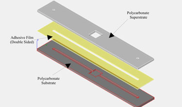
We demonstrate the use of double-sided adhesive films in the development of rapid prototype flow systems. These prototype fluidic devices have a great number of applications and since their preparation is a trivial matter, they may be prepared as and when required. Where there is a requirement for fluidic systems with a greater depth than the thickness of the film, multiple layers may be employed to expand the range of device depths obtainable.

What do I need?


  • ARCare 8725 double-sided adhesive (or similar)
  • Craft Knife, cutting board, template/ruler, etc.
  • Polycarbonate (or glass) slides with appropriately located inlet and outlet holes.

What do I do?


1. First, prepare the substrate and superstrate, cleaning both and locating any inlet and outlet connectors and / or holes as appropriate.

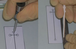
2. Prepare a template of the channel design required and transfer this to the backing tape of the adhesive film.

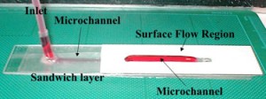
Figure 1. Sandwich-structure microfluidic device, illustrating internal and external flow control structures

3. Cut the adhesive film using the sharp craft knife, removing all traces of the template drawing, thereby leaving a double-sided adhesive film with missing segments corresponding to the desired flow system.

4. Adhere the film to the underside of the superstrate ensuring access to the inlet and outlet wells.

5. Remove the backing tape and attach the substrate slide, applying pressure to the system to assist adhesion process, creating a sandwich structure where the adhesive film defines the microfluidic system.

Figure 2. Sandwich-structure microfluidic device, filled with amaranth dye solution, enhancing the contrast of the internal and external flow control structures from the polycarbonate body of the device

The device shown in the Figures 1 and 2 combines an internal flow system with an external flow system, using multiple layers of the adhesive tape to define a flow profile on the upper surface of the chip, whilst maintaining fluid confinement.

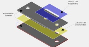
Figure 3. A cross-section of the device shown in Figures 1 & 2. Single- and double-sided adhesives can be used with polycarbonate slides to build multi-layer devices

Figure 3 shows a cross-section of the device. This system may also be utilised for the formation of devices where the channel is pre-defined in either the substrate or the superstrate, as shown in Figure 4.

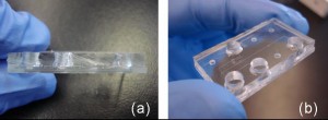
Figure 4. Sandwich-structure consisting of two polycarbonate slides, bonded using ARCare 8725 adhesive tape; microfluidic system defined in polycarbonate slide by CNC milling.

Figure 5 shows a cross-section of the device.

Figure 5. A cross-section of the device shown in Figure 4

What else should I know?


The method presented above is a useful technique in the preparation of flow systems for microfluidics work on a prototype scale. Whilst the limitations of the system are obvious in so far as pressure driven systems, where high pressure flow will result in rupture of the device, and the use of a silicon-based adhesive limits the applications for any systems requiring abrasive chemical or surface chemistry, it does provide ample opportunity to demonstrate a flow system, producing a working model in a very short space of time.

Digg This
Reddit This
Stumble Now!
Share on Facebook
Bookmark this on Delicious
Share on LinkedIn
Bookmark this on Technorati
Post on Twitter
Google Buzz (aka. Google Reader)

In-line microfluidic bubble trap

David T. Eddington
Department of Bioengineering, University of Illinois at Chicago, Chicago, IL

Why is this useful?


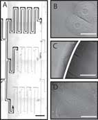
During long-term perfusion of microfluidic channels, bubbles sometimes enter and occlude the channel network as shown in Figure 1A.  In addition, bubbles are cytotoxic to mammalian cells as the surface tension of the air-liquid interface within a microfluidic channel is large enough to rupture cell membranes as shown in Figures 1B-D.  Even when care is taken to fill microfluidic networks and connect tubing without introducing bubbles (see the Tip “Avoiding bubble injection by droplet merging” by Young et al.), bubbles sometimes nucleate within the tubing and enter the channel network causing experiments to fail.  Traditional bubble traps are ineffective for microfluidic systems as these require tubing to connect the bubble trap to the microfluidic device which introduces more opportunities for bubbles to enter the channel network.  To reduce this problem an in-line microfluidic bubble trap has been developed that can be easily integrated into many microfluidic designs.

Figure 1

What do I need?


  • SU-8 mold master
  • PDMS (Sylgard 184, Dow Corning)
  • Razor blade
  • 5mm diameter x 5mm cylindrical spacer (can be adjusted depending on device design)

What do I do?


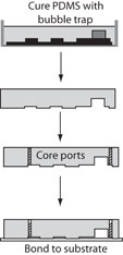
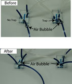
The fabrication of the microfluidic bubble trap is achieved by either molding a well within the network (Figure 2) or by cutting out a well after curing (Figure 3).  If a design is still being iterated, it is easier to cut out the bubble trap after curing.  However, if a final design has been reached, then molding the bubble trap into the network is ideal.  After the bubble trap is cut out or molded, the device is simply bonded to a substrate and when bubbles are introduced into the network they will enter the in-line bubble trap and float to the top as shown in Figure 4.  The volume of the bubble trap can be adjusted depending on the length of the experiments.

Figure 2

Iterated Design (Figure 2)

1. Cure PDMS on master.
2. After peeling the PDMS mold from the master, use the razor blade to cut out a bubble trap. The trap should be deep enough to allow the bubble to rise out of the microchannel.
3. Core access ports through the PDMS mold.
4. Assemble device.

Figure 3

Final Design (Figure 3)

1. Place stainless steel spacers on the master where bubble traps are desired.
2. Pour PDMS over master and cure.
3. After peeling the PDMS mold from the master, remove the steel spacer.  The spacer may need to be cut out of the mold with the razor blade.
4. Core access ports through the PDMS mold.
5. Assemble device.

Figure 4

References


E. W. K. Young, A. R. Wheeler and C. A. Simmons, Avoiding bubble injection by droplet merging, Chips & Tips (Lab on a Chip), 23 October 2006.

Digg This
Reddit This
Stumble Now!
Share on Facebook
Bookmark this on Delicious
Share on LinkedIn
Bookmark this on Technorati
Post on Twitter
Google Buzz (aka. Google Reader)

Rapid curing of PDMS for microfluidic applications

Adrian O’Neill, Jeffrey Soo Hoo and Glenn Walker
Joint Department of Biomedical Engineering, University of North Carolina-Chapel Hill and North Carolina State University

Why is this useful?


A new curing procedure is presented to expedite poly(dimethylsiloxane) (PDMS) microfluidic device fabrication. For microfluidic applications, PDMS is typically cured over a master in a plastic Petri dish at 80ºC for 2.5 hours. The curing temperature is limited by the maximum temperature a plastic Petri dish can withstand without warping. Dow Corning Sylgard 184 PDMS can be cured over a range of times and temperatures, spanning ~48 hours at room temperature to 10 minutes at 150ºC.  We present an alternate curing method, using an aluminium foil dish, that reduces the curing time from 2.5 hours to 10 minutes.

What do I need?


  • Aluminium foil, 0.001 inch thickness or greater
  • 90mm diameter crystallization dish (Pyrex 90 x 50mm)
  • PDMS (Dow Corning Sylgard 184)
  • Hotplate (Barnstead 721A digital hotplate)

What do I do?


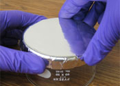
1. Cut a 4.5 inch diameter circle out of aluminium foil, being careful not to wrinkle the foil. Wrinkles may tilt the master causing the thickness of the PDMS mould to vary from one side of the design to the other.

Figure 1.

2. Form the foil over the bottom of the 90mm crystallization dish, as shown in Figure 1.

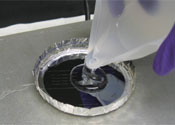
Figure 2.

3. After gently removing the foil, place the master in the foil dish and put the dish on a room temperature hotplate.

4. Mix the PDMS according to the manufacturer’s procedure [1].

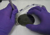
Figure 3.

5. Pour the desired amount of PDMS over the master, as shown in Figure 2.

6. Set the hotplate temperature to 150ºC. Once at 150ºC, cure the PDMS for 10 minutes.

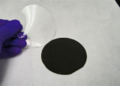
Figure 4.

7. Remove the foil dish from the hotplate and allow it to cool to room temperature.

8. Gently peel or cut the aluminium foil from the master and cut away any excess PDMS (Figure 3).

9. Finally, peel the PDMS mould from the master (Figure 4).

References


[1] Dow Corning Product Information, “Information about Dow Corning® brand Silicone Encapsulants,” 2005.

Digg This
Reddit This
Stumble Now!
Share on Facebook
Bookmark this on Delicious
Share on LinkedIn
Bookmark this on Technorati
Post on Twitter
Google Buzz (aka. Google Reader)