Archive for the ‘Nanoscale’ Category

Nanoscale 2014 Impact Factor released

We are thrilled to announce that Nanoscale’s latest impact factor has risen to 7.394 according to the 2014 Journal Citation Reports ®.

Thank you to all of the authors and referees who have contributed to our journal. Special thanks goes to our dedicated team of Editorial Board members without whom our continued success would not have been possible.

We invite you to join your peers and submit your best work to Nanoscale today.

Digg This
Reddit This
Stumble Now!
Share on Facebook
Bookmark this on Delicious
Share on LinkedIn
Bookmark this on Technorati
Post on Twitter
Google Buzz (aka. Google Reader)

HOT article: Design and assembly of supramolecular dual-modality nanoprobes

Self-assembled supramolecular nanoprobes

The synthesis of nanoprobes for application in more than one imaging technology is becoming more popular. So-called “bi-modal” probes can reduce limitations of single imaging modalities such as sensitivity or penetration depth. In this Hot article, the synthesis of two amphiphilic, dual-modality, optical imaging/MRI nanoprobes is reported. Each probe, containing both a fluorophore and a gadolinium complex, was specifically engineered using hydrophobic and hydrophilic components so they would self-assemble above the critical micelle concentration (CMC), which in turn would improve the MRI performance. The materials could offer potential advantages compared to conventional, unimolecular probes. Flow cytometry was used to confirm that both negatively charged assemblies were efficient at labelling KB-3-1 (human cervical cancer) cells at different labelling concentrations and incubation periods, through measurement of cell fluorescence. Cells viability was not compromised for each condition. The authors are now looking to further improve performance of self-assembled cell tracking agents through synthetic manipulation of construct size and surface charge.

Design and assembly of supramolecular dual-modality nanoprobes
Shuang Liu, Pengcheng Zhang, Sangeeta Ray Banerjee, Jiadi Xu, Martin G. Pomper and Honggang Cui
Nanoscale, 2015, 7, 9462-9466. DOI: 10.1039/C5NR01518A

Dr Mike Barrow is a guest web writer for the Nanoscale blog. He currently works as a Postdoctoral Researcher at the University of Liverpool.

Digg This
Reddit This
Stumble Now!
Share on Facebook
Bookmark this on Delicious
Share on LinkedIn
Bookmark this on Technorati
Post on Twitter
Google Buzz (aka. Google Reader)

Ready. Set. GO!

Graphene oxide (GO) is a versatile material with applications ranging from electronics to energy storage and biosensors. As a biosensing substrate, GO has many favorable attributes such as low cost, high signal-to-noise ratio, and the ability to efficiently quench fluorescence.

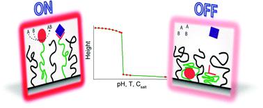
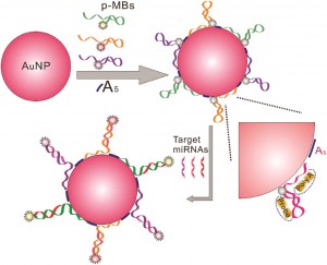
Scheme for the GO-aptamer based sensor for detection of thrombin.

This ability to quench fluorescence has inspired a range of biosensors using GO and Förster resonance energy transfer (FRET) for the sensitive detection of proteins using labelled probes, such as aptamers. However, the target proteins in such assays can non-specifically adsorb onto the surface of GO, thereby reducing the sensitivity.

To address this, Gao and co-workers implemented the use of polyethylene glycol (PEG) to prevent the non-specific adsorption of thrombin onto GO while implementing an aptamer-binding assay.  The authors report that the detection limit could be improved by optimizing the GO:PEG concentration. This manuscript helps to establish GO as promising tool in the biomedical and biotechnology fields.

Highly sensitive detection for proteins using graphene oxide-aptamer based sensors
Li Gao, Qin Li, Raoqi Li, Lirong Yan, Yang Zhou, Keping Chen and Haixia Shi
Nanoscale, 2015, Advance Article. DOI: 10.1039/C5NR01187F

Dr Lee Barrett is a guest web writer for the Nanoscale blog. Lee is currently a postdoctoral researcher in the Centre for Molecular Nanometrology at the University of Strathclyde. His research is currently focused on the development of nanoparticle-based sensors and surface enhanced Raman scattering (SERS). Follow him on Twitter @L_Bargie.

Digg This
Reddit This
Stumble Now!
Share on Facebook
Bookmark this on Delicious
Share on LinkedIn
Bookmark this on Technorati
Post on Twitter
Google Buzz (aka. Google Reader)

HOT article: Two-dimensional materials and their prospects in transistor electronics

Recently, the 50th anniversary of Moore’s law has been celebrated by the semiconductor industry. Although the current ITRS (International Technology Roadmap for Semiconductors) continues to propose “traditional” transistor materials such as Si and GaAs, attractive, two-dimensional alternatives have become visible on the horizon.

Schwierz et al. have recently published a Feature article in Nanoscale compiling the current knowledge on 2D materials. Their article focuses on the application of these as the channel material in field effect transistors.

According to the authors, two large trends can currently be observed: More Moore and More than Moore. The former utilizes well known semiconductors and improves performance by sophisticated manufacturing and scaling techniques. In contrast, the latter one employs compound semiconductors and novel alloys as 2D materials with a wide range of new properties.

Two-dimensional materials and their prospects in transistor electronics

The main material classes researched to date are explained further, covering X-anes, Fluoro-X-enes, TMDs (transition metal–chalcogen combinations), SMCs (semimetal–chalcogen combinations), MX-enes and (currently theoretical) group IV-IV and III-V 2D materials.

To assess the viability of the materials for applications within electronic circuits, Schwierz et al. also describe a wish list of ideal properties of next generation channel materials: bandgap, carrier mobility, heat conductivity, contact resistance and scale length. Based on experiences from established semiconductors, they also derive practical values needed for high performance FET.

The final part of the review examines the current status of the material classes. Notable performance records of well researched materials (e.g. 100 GHz graphene FET) as well as first demonstrators (e.g. first X-ane based FET) are given here. Finally, some arguments for a revival of silicon as a promising material for future applications are also given.

Two-dimensional materials and their prospects in transistor electronics
F. Schwierz, J. Pezoldt and R. Granzner
Nanoscale, 2015, 7, 8261-8283. DOI: 10.1039/C5NR01052G

Sebastian Axmann is a guest web-writer for the Nanoscale blog. His interests comprise manufacturing and metrology of nanostructures as well as their usage in current semiconductor devices. He also posts links to interesting research articles on Twitter: @SebastianAxmann.

Digg This
Reddit This
Stumble Now!
Share on Facebook
Bookmark this on Delicious
Share on LinkedIn
Bookmark this on Technorati
Post on Twitter
Google Buzz (aka. Google Reader)

HOT article: Photo-fluorescent and magnetic properties of iron oxide nanoparticles for biomedical applications

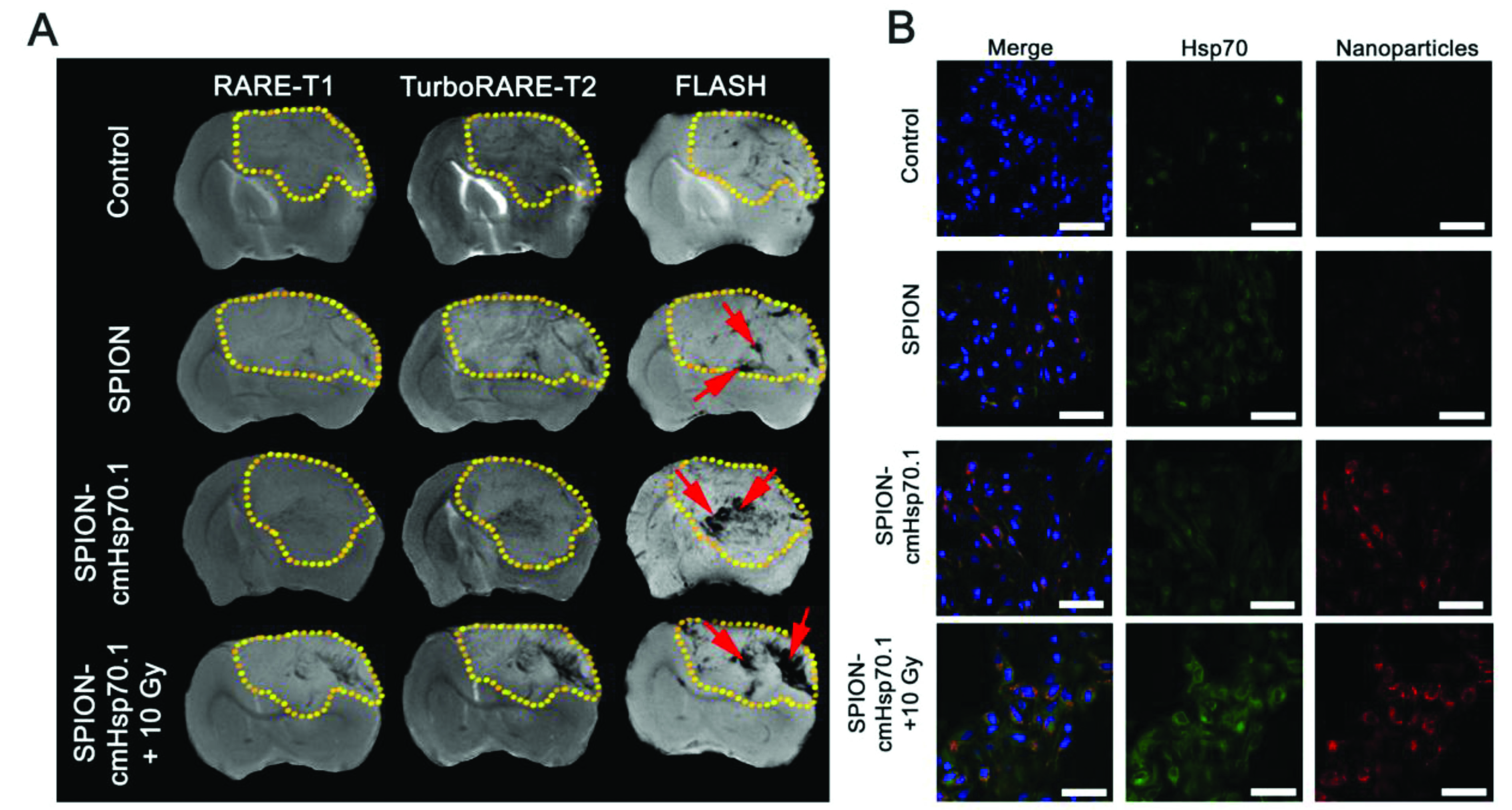
As cancer treatments evolve, focus has shifted to techniques and tools, which provide tumor-targeting capabilities and are uncoupled from common detrimental side effects.  The efficient delivery of new therapeutics has been a common area of interest, with studies focused on nanoparticle delivery systems being an eminent research area.

(a) TEM image of PS/Fe3O4 microspheres showing the amorphous coating entrapping multiple Fe3O4 nuclei. (b) TEM image of PAA/Fe3O4 and (c) cumulant size distribution of PAA/Fe3O4.

In this review article, Shi and co-workers draw attention to the properties of magnetite nanoparticles (Fe3O4), which can be utilised as customized therapeutics.  This review provides an overview of the synthesis of magnetite nanoparticles with an in-depth discussion related to their synthesis, functionalization and applications in a biological environment.

A highlight of this review includes an exploration into the recently discovered photo-luminescence properties of magnetite nanoparticles through studies of the electronic band structures to explain the emission mechanisms occurring.  The implications of thermal and magnetic induced hypothermia treatments utilizing these nanoparticles are also discussed relative to the patients being treated by such techniques.

From this review it can be determined that a new theragnostic platform has emerged with multi-functional capabilities both in terms of imaging and drug delivery.

Photo-fluorescent and magnetic properties of iron oxide nanoparticles for biomedical applications
Donglu Shi, M. E. Sadat, Andrew W. Dunn and David B. Mast
Nanoscale, 2015, 7, 8209-8232. DOI: 10.1039/C5NR01538C

Dr Derek Craig is a guest web writer for the Nanoscale blog. He is a Post Doctoral Research Fellow at the University of St. Andrews based in the fields of Biophotonics and Materials Science. With a background in chemistry, his work mainly focuses on the synthesis of nano to meso materials and the use of imaging techniques to study biological samples.

Digg This
Reddit This
Stumble Now!
Share on Facebook
Bookmark this on Delicious
Share on LinkedIn
Bookmark this on Technorati
Post on Twitter
Google Buzz (aka. Google Reader)

Single-walled carbon nanotubes: Catching some rays

Precision printing and optical modeling of ultrathin SWCNT/C60 heterojunction solar cells

Inexpensive photovoltaics (PV) are an attractive avenue of research in the field of solar cells. In particular, semi-conducting single-walled carbon nanotubes  (s-SWCNTs) are a promising photo-absorbing material due to their strong near-infrared (near-IR) absorption and high carrier mobility. However, most current production methods for SWCNT PVs suffer from high surface roughness and lack nanometer-scale deposition precision, thereby hampering the reproducibility of ultrathin PV devices.

To this end, the authors have utilized ultrasonic spraying in order to tune the thickness of s-SWCNT layers with nanometer-scale precision. The researchers have used a combination of atomic force microscopy (AFM) and optical profilometry to show that their ultrasonic spraying method produces smooth, uniform films with an average roughness of about 5 nm.  The advantage of this low roughness enables fabrication of s-SWCT/C60 bilayer devices with significantly thinner C60 layers than previously reported.

The results reported by the authors help to advance the production of low-cost PV devices by improving the performance and scalability of ultra-thin SWCNT-based solar cells. Ultra-thin SWCNTs reported here could find potential use in other emerging technologies such as vertical field effect transistors and light-emitting diodes incorporating s-SWCNT injection layers.

Precision printing and optical modeling of ultrathin SWCNT/C60 heterojunction solar cells
Sarah L. Guillot, Kevin S. Mistry, Azure D. Avery, Jonah Richard, Anne-Marie Dowgiallo, Paul F. Ndione, Jao van de Lagemaat, Matthew O. Reese and Jeffrey L. Blackburn
Nanoscale, 2015, 7, 6556-6566. DOI: 10.1039/C5NR00205B

Dr Lee Barrett is a guest web writer for the Nanoscale blog. Lee is currently a postdoctoral researcher in the Centre for Molecular Nanometrology at the University of Strathclyde. His research is currently focused on the development of nanoparticle-based sensors and surface enhanced Raman scattering (SERS). Follow him on Twitter: @L_Bargie.

Digg This
Reddit This
Stumble Now!
Share on Facebook
Bookmark this on Delicious
Share on LinkedIn
Bookmark this on Technorati
Post on Twitter
Google Buzz (aka. Google Reader)

HOT article: The support effect on the size and catalytic activity of thiolated Au25 nanoclusters as precatalysts

TEM images and size distribution (inset) of various Au25 (1 wt%)/support samples before and after 300 °C calcination.

The use of nanogold (Au NP) catalysts has been widely established for various applications including pharmaceuticals and perfumes.  However, their usage has been limited due to the conventional protocols employed for Au NP synthesis producing polydisperse size ranges, which have proven problematic for identifying catalytic active sites. Recently, this issue has been circumvented through instead using Au nanoclusters (Au NCs), which produce defined cluster sizes with well-defined physiochemical properties. As a direct consequence of being able to exert such control, there have been a number of applications established using such catalysts for processes including CO oxidation, and the oxidation of styrene and cyclohexane. However, whilst the role of the solid support is well established for Au NP catalysis, there currently exists a lack of knowledge on what effect/role the support plays in Au NCs catalysis.

In this study, Fang and co-workers report a systematic assessment of thiolated Au NCs on five different solid supports through examination of the size and electronic structure evolution of the Au NCs during heat treatment, and their catalytic performance when applied to the hydrogenation of nitrobenzene and oxidation of styrene.  The solid supports investigated include hydroxy-apatite (HAP), TiO2 (P25), activated carbon (AC), pyrolyzed grapheme oxide (PGO) and fumed SiO2.

The key findings of these studies establish that AuNCs on HAP and P25 supports presented enhanced activities over the other considered supports. This was found to be due to a number of factors, including reduced NC growth during calcination (heat treatment) following the removal of the thiolated ligands from the nanocluster surface. Further to this, the catalytic activity established during the hydrogenation of nitrobenzene and oxidation of styrene overwhelmingly showed that AuNC-HAP had a greater activity than any of the other supported catalysts. This was found to be due to both the reduced NC growth following heat treatment, and a change in the electronic structure of bound Au, resulting in strengthened metal support interactions.

Although this study has shown HAP to be a superior support in comparison to the others investigated, it should be noted that during heat treatment, an increase in the size of the nanoclusters was still observed.  As a consequence of this, the authors have objectively established improvements which should be made for future studies, including pursuing different support methods and improving the conditions under which the thiolated ligands can be removed from the Au NCs.

The support effect on the size and catalytic activity of thiolated Au25 nanoclusters as precatalysts
Jun Fang, Jingguo Li, Bin Zhang, Xun Yuan, Hiroyuki Asakura, Tsunehiro Tanaka, Kentaro Teramura, Jianping Xie and Ning Yan
Nanoscale, 2015, 7, 6325-6333. DOI: 10.1039/C5NR00549C

Dr Derek Craig is a guest web writer for the Nanoscale blog. He is a Post Doctoral Research Fellow at the University of St. Andrews based in the fields of Biophotonics and Materials Science. With a background in chemistry, his work mainly focuses on the synthesis of nano to meso materials and the use of imaging techniques to study biological samples.

Digg This
Reddit This
Stumble Now!
Share on Facebook
Bookmark this on Delicious
Share on LinkedIn
Bookmark this on Technorati
Post on Twitter
Google Buzz (aka. Google Reader)

Poster prize winner at PhoBiA Annual Nanophotonics International Conference (PANIC 2015)

Maciej Bieniek receiving the Nanoscale prize for the best oral presentation at PANIC 2015

Many congratulations to Maciej Bieniek for winning the Nanoscale prize for the best oral presentation at the PhoBiA Annual Nanophotonics International Conference (PANIC 2015).

Maciej, from the Wrocław University of Technology, was chosen by Professors Isabelle Ledoux-Rak, Luana Persano and Robert Luxenhofer to receive the prize for his oral presentation entitled “Two-dimensional topological insulator quantum dots”.

The 6th PhoBiA Annual Nanophotonics International Conference took place from 20th to 23rd April 2015 at Wroclaw University of Technology (Poland). The interdisciplinary conference aims to gather students and young scientists working in the fields of photonics, nanotechnology, biotechnology, materials science and organic electronics in order to enable them to discuss and share their knowledge. The event, organised by students, also featured a number of invited speakers. Further details are available on the conference website.

Nanoscale will be awarding more prizes throughout the year – keep an eye out to find out about the winners!

Digg This
Reddit This
Stumble Now!
Share on Facebook
Bookmark this on Delicious
Share on LinkedIn
Bookmark this on Technorati
Post on Twitter
Google Buzz (aka. Google Reader)

6th International Conference on Nanoscience and Technology (ChinaNANO 2015)

ChinaNANO 2015

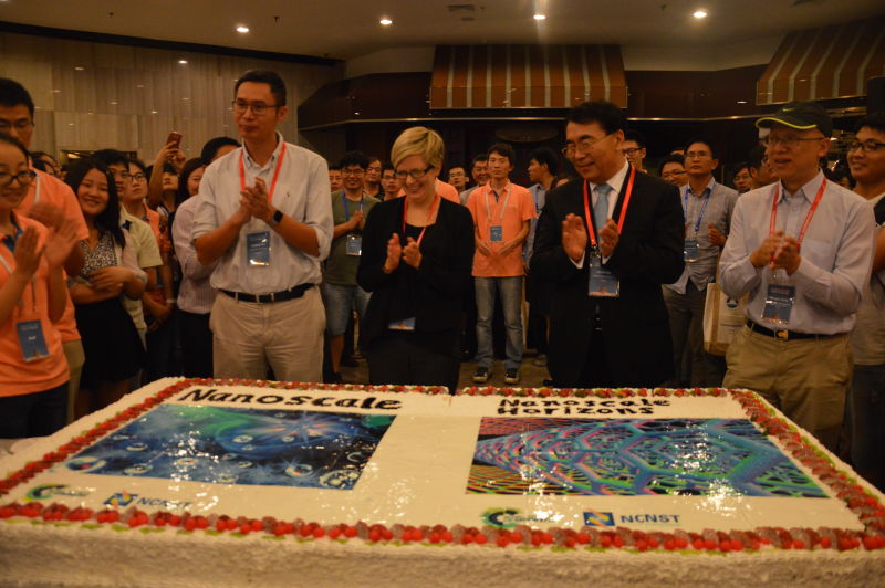
Nanoscale is proud to collaborate with the 6th International Conference on Nanoscience and Technology (ChinaNANO 2015), which will be held at the Beijing International Convention Center in Beijing, China on 3-5 September 2015. The conference is organised by the National Center for Nanoscience and Technology, China. Professor Chunli Bai will act as the Chairman of the organising committee.

ChinaNANO 2015 aims to stimulate discussions on the forefront of research in nanoscience and nanotechnology, focusing on the following topics: carbon nanomaterials, inorganic nanomaterials and MOFs, self-assembly and supramolecules, nanocomposites and applications, energy and environmental nanotechnology, nanophotonics and optoelectronics, nanodevices and nanosystems, nanobiotechnology and nanomedicine, nanocharacterization and metrology, modelling and simulation of nanostructures, and the environment, safety and health of nanomaterials.

Submit your abstract now – the deadline is 30 April 2015. For more information, please see the conference website.

Digg This
Reddit This
Stumble Now!
Share on Facebook
Bookmark this on Delicious
Share on LinkedIn
Bookmark this on Technorati
Post on Twitter
Google Buzz (aka. Google Reader)

Disrupting graphene

Scientists across the field of 2D materials have put forward a roadmap to steer graphene research off the drawing board, to a point where it emerges within disruptive technologies that alter people’s lives the world over.

The roadmap is split into 11 science and technology themes including spintronics, biomedical devices and energy conversion and storage. Short-, medium- and long-term targets for technological milestones as well as safety profiles sit alongside the plethora of potential applications.

Interested? Read the full story by Harriet Brewerton in Chemistry World.

The original article is free to access and can be read at:

Andrea C. Ferrari, Francesco Bonaccorso, Vladimir Fal’ko, Konstantin S. Novoselov, Stephan Roche, Peter Bøggild, Stefano Borini, Frank H. L. Koppens, Vincenzo Palermo, Nicola Pugno, José A. Garrido, Roman Sordan, Alberto Bianco, Laura Ballerini, Maurizio Prato, Elefterios Lidorikis, Jani Kivioja, Claudio Marinelli, Tapani Ryhänen, Alberto Morpurgo, Jonathan N. Coleman, Valeria Nicolosi, Luigi Colombo, Albert Fert, Mar Garcia-Hernandez, Adrian Bachtold, Grégory F. Schneider, Francisco Guinea, Cees Dekker, Matteo Barbone, Zhipei Sun, Costas Galiotis, Alexander N. Grigorenko, Gerasimos Konstantatos, Andras Kis, Mikhail Katsnelson, Lieven Vandersypen, Annick Loiseau, Vittorio Morandi, Daniel Neumaier, Emanuele Treossi, Vittorio Pellegrini, Marco Polini, Alessandro Tredicucci, Gareth M. Williams, Byung Hee Hong, Jong-Hyun Ahn, Jong Min Kim, Herbert Zirath, Bart J. van Wees, Herre van der Zant, Luigi Occhipinti, Andrea Di Matteo, Ian A. Kinloch, Thomas Seyller, Etienne Quesnel, Xinliang Feng, Ken Teo, Nalin Rupesinghe, Pertti Hakonen, Simon R. T. Neil, Quentin Tannock, Tomas Löfwander and Jari Kinaret
Nanoscale, 2015, 7, 4598-4810. DOI: 10.1039/C4NR01600A
Digg This
Reddit This
Stumble Now!
Share on Facebook
Bookmark this on Delicious
Share on LinkedIn
Bookmark this on Technorati
Post on Twitter
Google Buzz (aka. Google Reader)