 From stochastic single atomic switch to nanoscale resistive memory device
Attila Geresdi, András Halbritter, András Gyenis, Péter Makk and György Mihály
Nanoscale, 2011, DOI:10.1039/C0NR00951B
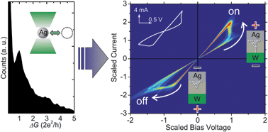
Scientists from Hungary have published some important work in Nanoscale regarding the use of solid state ionic conductors as atomic-sized junctions in non-volatile computer memory devices. By varying the size of the junctions from single-atom-sized to 10 nm, the group concluded that there is a lower size limit of 3 nm for reliable ionic nano-switches, a size which is well below the resolution of recent lithographic techniques.
In this work, Garesdi et al. created the junctions by gently touching a silver thin film with an electrochemically sharpened tungsten tip. Exposure of the silver film to air established the ionic conductor surface layer, and the nanoscale ‘point-contact’ geometry was sufficient to form a reliable switching device above the 3 nm threshold. Below this value, the switching process was much less reliable. The storage density here, even with the 3 nm limit, would be higher than current NAND flash devices and similar to the proposed bit size threshold of magnetic media which arises due to the superparamagnetic limit.
The authors provide a detailed analysis of the physical properties of the nano-junctions, as well as an explanation of the underlying mechanisms. They conclude that their ionic conductor-based devices are good candidates for non-volatile memory cells.
To read this article, click here.
From stochastic single atomic switch to nanoscale resistive memory device
Attila Geresdi, András Halbritter, András Gyenis, Péter Makk and György Mihály
Nanoscale
DOI:10.1039/C0NR00951B
Scientists from Hungary have published some important results in Nanoscale regarding the use of solid state ionic conductors as atomic-sized junctions in non-volatile computer memory devices. By varying the size of the junctions from single-atom-sized to 10 nm, the group concluded that there is a lower size limit of 3 nm for reliable ionic nano-switches, a size which is well below the resolution of recent lithographic techniques.
In this work, Garesdi et al. created these junctions by gently touching a silver thin film with an electrochemically sharpened tungsten tip. Exposure of the silver film to air established the ionic conductor surface layer, and the nanoscale ‘point-contact’ geometry was sufficient to form a reliable switching device above the 3 nm threshold. Below this value, the switching process was much less reliable. The storage density here, even with the 3 nm limit, would be higher than current NAND flash devices and similar to the proposed bit size limit of magnetic media which arises due to the superparamagnetic limit.
The authors provide a detailed analysis of the physical properties of the nano-junctions, as well as an explanation of the underlying mechanisms. They conclude that their ionic conductor-based devices are good candidates for non-volatile memory cells.
To read this article, click here.


