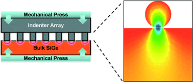
The first articles that include the new Design, System, Application box have now been published online!
The common theme running through all articles in Molecular Systems Design & Engineering is a problem solving strategy or vision based on molecular-level design or optimisation (be it through theory, modelling or experiment) leading to desired systems-level functionality and performance. We hope that many articles will present methodologies that will guide and stimulate ideas across disciplines.
The Design, System, Application box gives authors the chance to explain their molecular design strategy in general terms so readers can be inspired by its ideas. This text should also set work in the context of a wider development story by emphasising the desired systems functionality and application potential. Please see the journal specific guidelines for more details.
Take a look at this example from the paper “Modeling and simulation of compositional engineering in SiGe films using patterned stress fields” by Daniel Kaiser, Swapnadip Ghosh, Sang M. Han and Talid Sinno.
In this work the authors model atomic diffusion under mechanical stress, which can be used to determine the process parameters needed to create structures in SiGe films exhibiting quantum confinement. The model enables optimisation to create specific structures for device applications. This is an important addition to the molecular engineer’s toolbox and the authors do a great job of explaining the concept and its potential in their Design, System, Application statement:
| Design, System, Application
Semiconductor nanostructures exhibiting quantum confinement are at the heart of numerous existing optoelectronic technologies, such as lasers and detectors. They are also potentially a route for building future devices for quantum computing, cryptography and ultra-high density information storage. A key obstacle to realizing this potential is the ability to fabricate large numbers of such nanostructures on semiconductor substrates with a high degree of spatial and size uniformity. Here, we describe and deploy a predictive multiresolution model for describing atomic diffusion in the presence of mechanical stress in the silicon–germanium alloy system over large length and timescales. The model is used to investigate processing avenues for creating highly structured, nanoscale compositional profiles in silicon–germanium substrates consistent with the quantum confinement properties required for next-generation optoelectronic devices. Specifically, we study a process in which a patterned template of nanoindenters is pressed against the alloy substrate, thereby inducing structured stress fields that manipulate atomic diffusion to create desired compositional gradients. The model is used to probe the impact of select parameters in the high-dimensional process space, such as indenter shape, size, and spacing. Future process optimization will provide guidelines for creating compositional profiles targeting a wide range of device requirements. |


