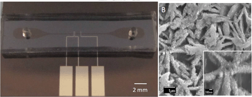
A new method for the direct, bottom-up growth of a SERS substrate within a microfluidic channel, developed at the University of Connecticut, will enable the inexpensive fabrication of SERS-integrated devices.
Surface enhanced Raman scattering (SERS) spectroscopy is a powerful method for analyte detection and identification. SERS relies on the electric field enhancement provided by nanostructured metal surfaces to amplify the Raman scattering “fingerprint” of adsorbed molecules, enabling specific detection down to the single molecule level1. Previously, SERS integration into practical devices has been limited, partly due to the cost and difficultly of fabricating SERS substrates and microfluidic channels separately, then aligning and bonding them together. In this HOT article, researchers at the University of Connecticut led by Prof. Yu Lei have devised a method to fabricate a novel nanostructured SERS substrate directly within existing microfluidic channels, greatly simplifying the construction of such devices2.
Previous SERS-integrated microfluidic devices have utilized silver plates fabricated via laser writing3 and silver nanoparticles created using physical vapor deposition4 as SERS substrates. These devices provide high detection sensitivity, but are costly to produce due to the top-down fabrication methods used. The advantage of the new method by Parisi et al. is the ability to synthesize a SERS substrate bottom-up and in situ, reducing the complexity and cost of device fabrication. SERS experiments can then be carried out immediately.
In situ electrodeposition and galvanic displacement are used to fabricate a nanostructured SERS substrate (right) within a microfluidic device (left)
In the new technique, copper nanowalls coated with carbon are synthesized inside a microfluidic channel via electrodeposition. This is accomplished by applying a voltage across part of the channel while copper acetate flows through. Next, silver nitrate flows through the channel, and a galvanic replacement reaction results in silver nanoparticles coating the nanowalls. Then, an analyte solution flows through the channel and adsorbs onto the substrate, allowing the user to measure SERS. The authors used crystal violet as an example analyte to demonstrate the sensitive in-channel detection capability, measuring the SERS of analyte concentrations down to 50 pM.
The researchers hope that their fabrication technique will ultimately allow SERS to be integrated into various microfluidics-based biological and chemical sensing platforms, increasing the power and flexibility of these devices.
References
1. J. Kneipp et al., Chem. Soc. Rev., 37, 1052–1060, 2008.
2. J. Parisi et al., Lab on a Chip, 13, 1501–1508, 2013.
3. B.-B. Xu et al., Lab on a Chip, 11, 3347–3351, 2011.
4. Z. Geng et al., Sensors and Actuators A, 169 (1), 37–42, 2011.
Read this HOT article in Lab on a Chip today:
In situ synthesis of silver nanoparticle decorated vertical nanowalls in a microfluidic device for ultrasensitive in-channel SERS sensing
Joseph Parisi, Liang Su and Yu Lei
DOI: 10.1039/C3LC41249K
This article is featured in the web collection Lab on a Chip Top 10%
Katie Mayer is a post-doctoral researcher in the Walt Laboratory at Tufts University, USA


