Easy and robust interconnection methods for PDMS-based microfluidics

Shuo Wang, Huaiqiang Yu, Wei Wang and Zhihong Li present a useful method to prevent PDMS cracking during the sealing of chips

Shuo Wang, Huaiqiang Yu, Wei Wang and Zhihong Li
National Key Laboratory of Science and Technology on Micro/Nano Fabrication, Institute of Microelectronics, Peking University, China

Why is this useful?


PDMS (polydimethylsiloxane) is one of the most important materials in microfluidics and is widely used because of its optical transparency, ease-in-fabrication, low cost and air permeability. A widely used interconnection approach for PDMS chips is the “press-fit” method [1]. However, the seal is only achieved by the compression of PDMS. An unexpected disturbance to the needle may damage the PDMS around it and produce small cracks leading to leakage around the needle. The mechanism of disturbance-caused leakage is shown in Fig. 1.

Fig. 1 Mechanism of disturbance-caused leakage

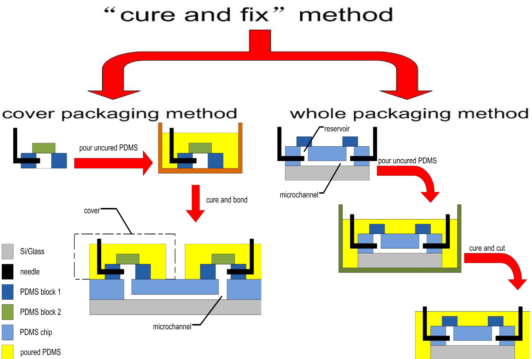
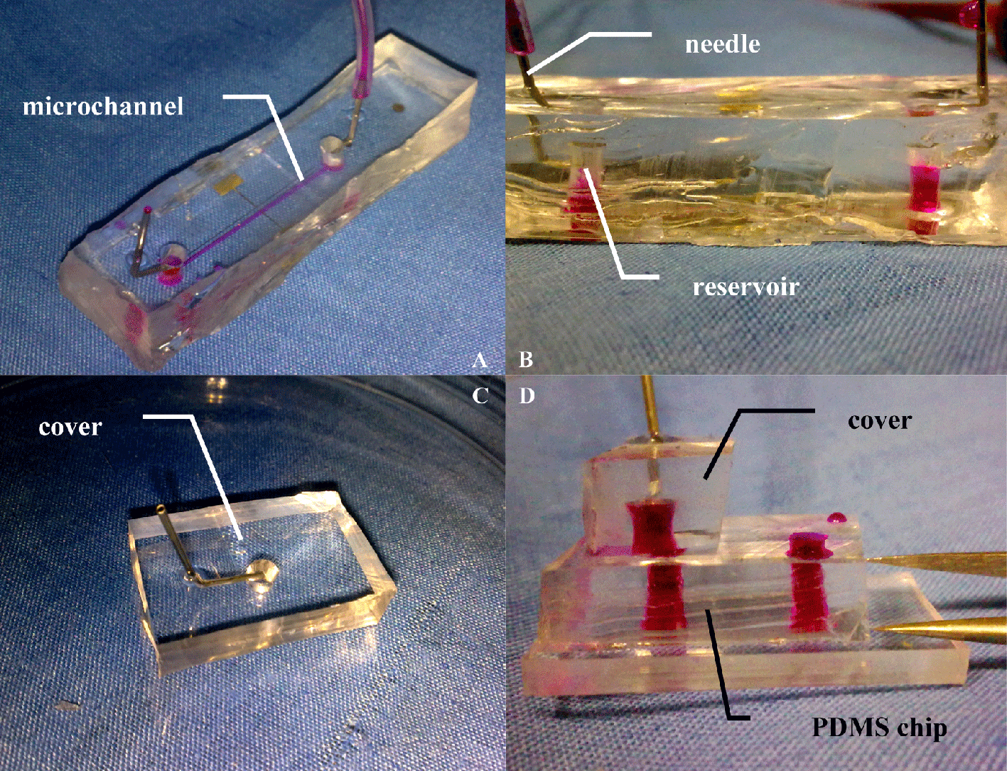
Here, we report two easy methods of fixing needles by a secondary PDMS fabrication. In these “cure and fix” methods, uncured PDMS is poured and cured to fix needles. Sectional views in Fig. 2 show the two schematic fabrication processes respectively. Cover packaging methods can be applied to produce covers in large number used as standard components. After PDMS chips are made, simply bond them with these standard covers to seal reservoirs. We can also employ whole packaging method to fabricate one specific device with lots of reservoirs.

Fig. 2 “Cure and fix” method

What do I need?


  • PDMS chip peeled off from Si mould
  • Uncured PDMS (base:cure = 10:1)
  • Silicon or glass substrate
  • Unmodified needles
  • Scalpel and tweezers
  • Hole puncher
  • Oxygen plasma etching machine or corona charging device

How do I do it?


Whole packaging method

  1. Punch holes for reservoirs on a PDMS chip and bond the chip with silicon or glass substrates using oxygen plasma or corona treatment [2].
  2. Plunge unmodified needles into reservoirs laterally using the “press-fit” method. Clear away PDMS scraps with a pair of tweezers.
  3. Seal all reservoirs by bonding PDMS blocks. Cast uncured PDMS onto the chip until lower half of the needle is submerged.
  4. After curing PDMS at 70°C for 1 hour, cut the chip into proper size.

Cover packaging method

  1. Punch a hole for the reservoir on a flat PDMS block and bond it with another PDMS block
  2. Plunge an unmodified needle into the reservoir laterally using the “press-fit” method. Clear away PDMS scraps with a pair of tweezers.
  3. Put the PDMS cover on a flat culture dish and cast uncured PDMS.
  4. After curing PDMS at 70°C for 1 hour, cut the cover into proper size.
  5. Bond the cover with a PDMS chip to seal reservoirs.

What else should I know?


In order to plunge the unmodified needle into reservoirs successfully, the PDMS cannot be too thin. The thickness should be larger than 3 mm.
Be careful in step 4 of whole packaging method because silicon and glass are brittle.

Fig. 3 A) Vertical view and B) side view of device using whole packaging method C) vertical view and D) side view of device using cover packaging method

References


[1] A. M. Christensen, D. A. Chang-Yen and B. K. Gale, Characterization of interconnects used in PDMS microfluidic systems. J. Micromech. Microeng., 2005, 15, 928-934.
[2] K. Haubert, T. Drier and D. Beebe, PDMS bonding by means of a portable, low-cost corona system, Lab Chip, 2006, 6, 1548-1549.

Digg This
Reddit This
Stumble Now!
Share on Facebook
Bookmark this on Delicious
Share on LinkedIn
Bookmark this on Technorati
Post on Twitter
Google Buzz (aka. Google Reader)

Have you seen our new Facebook page?

Chips & Tips has a shiny new Facebook page!

Like us and join the discussion, we’d love to hear your tips for chips!

Digg This
Reddit This
Stumble Now!
Share on Facebook
Bookmark this on Delicious
Share on LinkedIn
Bookmark this on Technorati
Post on Twitter
Google Buzz (aka. Google Reader)

Adding colour to PMDS chips for enhanced contrast

Marco A. Cartas-Ayala and Suman Bose introduce a method for dying PDMS

Marco A. Cartas-Ayala and Suman Bose
Department of Mechanical Engineering, Massachusetts Institute of Technology, USA.

Why is this useful?


Most materials used to fabricate microfluidic devices are transparent to facilitate sample visualization (e.g. PDMS), but this property has several drawbacks too. Alignment and visualization of the channels is difficult when the channels are completely transparent, making bonding of polymer devices difficult. Additionally, when multilayer polymer devices are manufactured, sometimes it is necessary to distinguish between different layers to easily evaluate functionality. Finally, having a way to add permanently colour to any kind of transparent channel can become really handy when creating permanent exhibitions displaying the devices created in the lab.

What do I need?


  1. PDMS (Sylgard 184)
  2. SILC PIG. blue silicone pigment, from Smooth-On, Inc
  3. 3 mL Syringe
  4. Blunt pieces of stainless tube (1/2 inch long, diameter smaller than PDMS holes, from New England Small Tube)
  5. Tygon tubing that fits the blunt needles and the stainless pieces of tubing
  6. Blunt needles for 1 mL syringe (diameter selected accordingly to tygon tubing diameter)

What do I do?


  1. Mix PDMS (Sylgard 184) in the recommended 10:1 ratio
  2. Add to the mix 5% w/w of the rubber paint and mix completely. If the mixture is not mixed thoroughly, pockets of paint can be formed in the final mixture, if you have problems with the mix, reduce the paint ratio
  3. Degas the mixture for 30 minutes
  4. Load 0.1 mL of the sample into the syringe with the blunt needle and tubing
  5. Inject into the channels to visualize. Be careful to not introduce bubbles, while air in PDMS leaks out when enough pressure is applied, air has to be flown out from glass devices
  6. Cure PDMS at 70 C for 1 hour
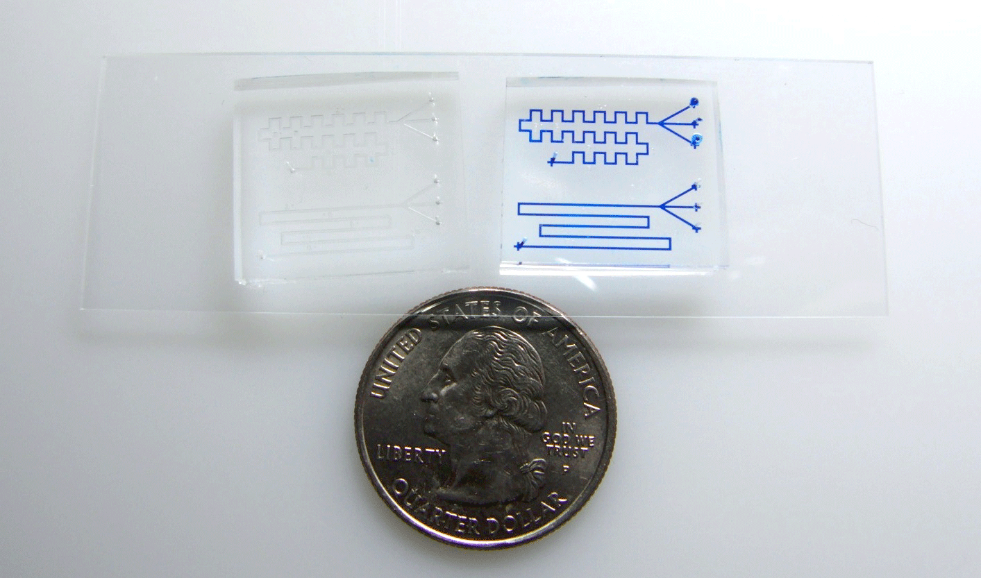
  7. Devices are ready for display. Notice the enhanced contrast of the colour filled channels vs the empty channels for the same device in Figure 2. While channels are visible only from some directions when they reflect light, colour-PDMS devices can be observed from every direction. Additionally, different device layers or areas can be specified by colour. In the figure control layers are blue and flow layers are red

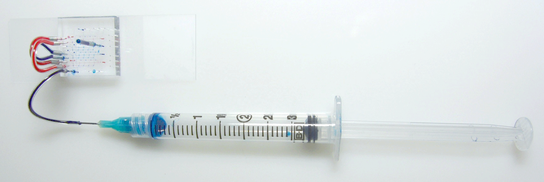
Fig. 1 Injection of PDMS through the channels. Air trapped inside the syringe provides a way to regulate the pressure applied to the device to minimize de-bonding. Compressing the air to 1/3 of original volume should provide enough pressure to drive the PDMS through.


Fig. 2 Enhanced channel contrast after injection, devices on the left side have empty channels and devices on the right have color PDMS inside.

Fig. 3 Different device zones can be identified by color. Here control layer is blue and flow layer is red. Secondary regulation channels are practically invisible when not filled.

References


[1] http://www.upchurch.com
[2] http://www.smooth-on.com

Digg This
Reddit This
Stumble Now!
Share on Facebook
Bookmark this on Delicious
Share on LinkedIn
Bookmark this on Technorati
Post on Twitter
Google Buzz (aka. Google Reader)

A simple microfluidic 4-way valve by clamping interconnected tubing

Boyang Zhang, Milica Radisic and Shashi Murthy describe a simple 4-way valve that overcomes the problem of large dead volumes in commercial valves

Boyang Zhang1, Milica Radisic1, Shashi Murthy2
1Department of Chemical Engineering and Applied Chemistry, University of Toronto, Toronto, ON, Canada
2Department of Chemical Engineering, Northeastern University, Boston, MA, USA

Background


The operation of microfluidic systems often requires sequential injection of more than one type of solution with a syringe pump. For instance, many adhesion-based cell-separation devices require additional injection of washing buffer or/and cell-releasing buffer after cell injection [1, 2]. Minimal flow disturbance to the system during switching to the next solution is critical for proper operation of such devices. Switching syringes during pumping will inevitably stop the flow and risk introducing bubbles to the device. Simple four-way valves are traditionally used in such cases [3]. However, many commercially available four-way valves have large dead volumes and long residence times that make them incompatible with microfluidic systems.

Why is this useful?


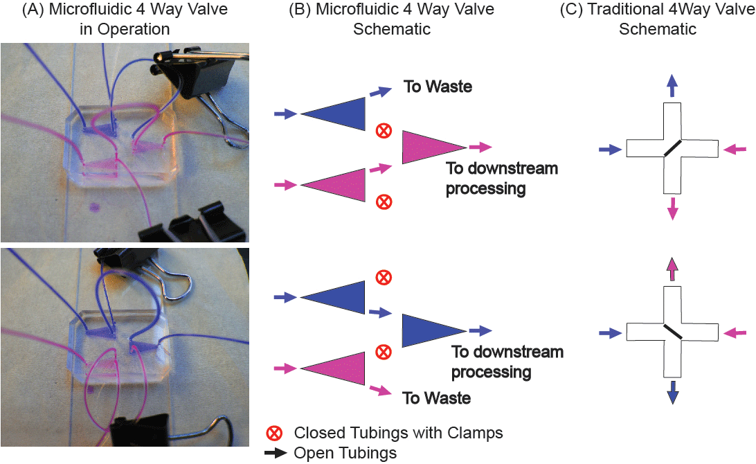
Here we present a simple, three-chamber microfluidic system with interconnected tubings (Figure 1) as an alternative to the traditional 4-way valve used for switching between solutions during experiments. For microfluidics applications, our system has the advantages of (1) allowing for switching between two solutions with minimal disturbance to the flow, (2) greatly reduced risk of introduction of unwanted air bubbles into the system, and (3) greatly reduced dead volume. The total volume of our system is two orders of magnitude less than a typical, commercially available 4-way valve (~1 µL as compared to ~1 mL) [5]. Our valve system is simple and cost-effective, as it utilizes clamps (binder clips) to block selected tubings. We have also shown that the tubings are strong enough to withstand several iterations of clamping and release. Lastly, this method can be scaled up to control the flow of more than two types of solutions, simply by adding more chambers and clamps.

What do I need?

  • Clamps (Binder Clips)
  • Tygon tubing (any size)
  • PDMS silicone elastomer base and curing agent (Sylgard 184, Dow Corning)
  • Glass slides, pre-cleaned (Fisher Scientific, 75mm x 50mm x 1mm, Cat. No. 12-550-C)
  • Scotch tape (3M Scotch® Transparent Tape 600)

What do I do?


(1)  Fabricate the master for the device. The device includes three triangular shaped chambers. The exact dimensions of these chambers are not critical and should be tailored to the specific experiment. In this case, triangular shaped channel with height of 40 μm and edge-width of 3 mm is used for flow rate up to 80 μl/min. The master can be fabricated with scotch tape which would greatly speed up the fabrication step especially for design with only large features [4].

(1)  Pour PDMS over the master and cure to create a PDMS-based device.

(2)  Drill holes as indicated in Figure 1 and bond the device to a glass slide.

(3)  Insert the tubing into the holes, again following Figure 1.

(4)  Fill the device with selected solution and clamp shut the selected tubing.

(5)  To switch solutions during an experiment, simply switch the position of the clamps as shown in Figure 1.

Figure 1. Device schematic: (A) Microfluidic 4 way valve with color dyes to demonstrate the function of the clamps to stop and re-route flows. (B) Schematic of the device in operation. (C) Traditional concept of 4 way valves.

References


1. B. D. Plouffe, M. A. Brown, R. K. Iyer, M. Radisic and S. K. Murthy, Controlled capture and release of cardiac fibroblasts using peptide-functionalized alginate gels in microfluidic channels, Lab Chip, 2009, 9, 1507-10.
2. B. D. Plouffe, M. Radisic and S. K. Murthy, Microfluidic depletion of endothelial cells, smooth muscle cells, and fibroblasts from heterogeneous suspensions, Lab Chip, 2008, 8, 462-72.
3. L. Kim, M. D. Vahey, H.-Y. Lee and J. Voldman, Microfluidic arrays for logarithmically perfused embryonic stem cell culture, Lab Chip, 2006, 6, 394-406.
4.  A. B. Shrirao and R. Perez-Castillejos, Simple Fabrication of Microfluidic Devices by Replicating Scotch-tape Masters, Chips & Tips (Lab on a Chip), 17 May 2010.
5. 4 WAY ACTUATION VALVES, Parker Hannifin Corp, 04 October 2011.

Digg This
Reddit This
Stumble Now!
Share on Facebook
Bookmark this on Delicious
Share on LinkedIn
Bookmark this on Technorati
Post on Twitter
Google Buzz (aka. Google Reader)

Drilling inlet and outlet ports in brittle substrates

R.J. Shilton, L. Y. Yeo, and J. R. Friend show how to easily drill holes for ports in microfluidic devices, even with brittle substrates

R.J. Shilton, L. Y. Yeo, and J. R. Friend
MicroNanophysics Research Laboratory, Department of Mechanical and Aerospace Engineering, Monash University, Clayton, Victoria, 3800, Australia

Purpose


It is often necessary to form millimeter order holes in glass (and similar) substrates to form inlet or outlet ports in microfluidic devices. The easiest way to do this is to simply drill a hole in the required position, however owing to the brittle nature of most materials used in these devices, this can often lead to a high failure rate where the devices crack during the drilling process. Outlined here is a simple procedure for drilling ports in microfluidic devices, which has been tested with glass, silicon, and lithium niobate, with a very high success rate.

Materials


  • ~ 1mm diamond drill bit (UKAM Industrial Superhard Tools, Valencia, CA)
  • Drill press
  • Double sided tape
  • Disposable plastic petri dish
  • Small piece of alumina (or other hard flat material)
  • Substrate to drill ports into

Procedure


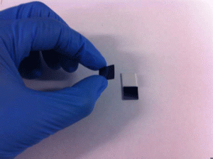
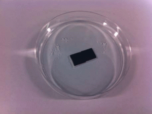
1. Attach microfluidic device to alumina with double sided tape. We have used this method reliably to drill ports in glass, silicon, and lithium niobate, however in principle it should work on a range of similar substrates. Silicon is shown in all images.

2.  Stick alumina to bottom of petri dish with a small amount of double sided tape.

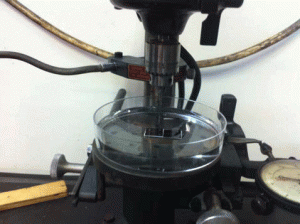
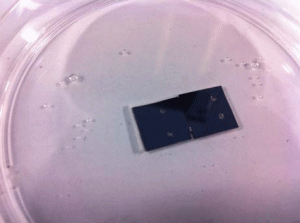
3. Fill petri dish with a generous amount of water to cool down the drill site, and to remove particles into the fluid while drilling the hole.

4. Attach diamond drill bit to drill press. We successfully used drill bits of diameter 0.75 and 1 mm, however others should work equally as well.

5. Drill at a high speed (~10,000 RPM). Quite a bit of force can be applied without cracking the substrate, as it is stuck to a rigid backing. Drilling through a 0.5 mm thick substrate should take about ten to fifteen seconds, if it is attached firmly.


What else should I know?


  • Release the downward force a little near the hole exit, to avoid a rough hole on the other side.
  • Keep device immersed in water after drilling until it is ready to be cleaned to avoid particles becoming stuck in device channels etc…
  • Change water regularly to remove particle build up

MicroNanophysics Research Laboratory,

Department of Mechanical and Aerospace Engineering,

Monash University, Clayton, Victoria, 3800, Australia

Digg This
Reddit This
Stumble Now!
Share on Facebook
Bookmark this on Delicious
Share on LinkedIn
Bookmark this on Technorati
Post on Twitter
Google Buzz (aka. Google Reader)

Simple and inexpensive macro to microfluidic interface connectors for high pressure applications

Sopan Phapal, Tuhina Vijay and P. Sunthar present an easy and inexpensive way to produce a glue-free macro to micro interface connector which can withstand high pressures

Sopan M. Phapal, Tuhina Vijay and P. Sunthar
Chemical Engineering Department, Indian Institute of Technology Bombay, Powai-400 076, India.

Why is this useful?


There are several ways to connect macro to micro interfaces (e.g., from syringe pump to microfluidic chip) in the miniaturization field. The ideal connector should withstand very high pressure and not leak. Commercially available Nanoports are often used as connectors but they are expensive, sometimes become clogged when glue is used, and cannot be reused. In this tip we present an easy and inexpensive way to produce a macro to micro interface connector which can withstand high pressure and is glue free.

What do I need?


•    2.5 ml plastic BD syringe with Luer-Lok (Luer tip ID at back 2.33 mm/0.095”; front ID 1.75 mm/0.07”)
•    16G SS needles (OD= 1.65  mm/0.065”)
•    Grinder with hard abrasive disk to cut/ blunt the needles
•    16G PTFE tubing, Hamilton, Cat No.20916 ; OD=1.9 mm/0.075”; ID=1.2 mm/0.047”[1]
•    Surgical knife/cutter to cut the Luer part of the syringe
•    Glue (Araldite).

A syringe contains a male Luer part and the needle head is its counter female Luer part. There are two types of Luer fittings, one Luer-slip which when pressed together, fits in each other by friction; and the other is Luer-Lok which has threads in the male part and the female part (needle head) screws in to it (Figure 1). We used both Luer-slip and Luer-Lok syringe tips, but the Luer-Lok is better for high pressure application.

Figure 1. A syringe with a male Luer-Lok connection fitting (threaded) and a needle head with female Luer-Lok fitting (purple) which screws into it.

What do I do?


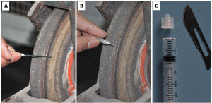
1. Make the needles blunt with the help of grinder (Fig. 2A & B). Cut the Luer-Lok tip of the plastic syringe with a sharp blade/cutter (Fig. 2C).

Figure 2.

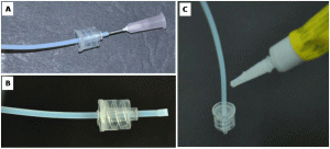
2. Prepare the male Luer part. Insert the PTFE tube (OD= 1.9mm) into Luer-Lok tip (back ID= 2.3 mm and front ID is 1.75 mm) as shown in Fig. 3A. Now heat the 16G SS blunt needle and insert it into the PTFE tube up to some mm and remove it (Fig. 3B). Because of this, the tip of the tube becomes wider than Luer-Lok ID, fitting tight mechanically. Pull the Luer-Lok up to the wide tip of PTFE tube and place a drop of araldite at the back side of it (Fig. 3C). This will cause a tight fit of the Luer-Lok tip with the PTFE tube.

Figure 3.

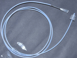
3. Preparation of the female Luer part. Heat the 16G SS blunt needle (OD= 1.65 mm) and insert it into 16G PTFE tube (ID=1.2mm), as shown in Fig. 4. As the needle OD is bigger than tube ID, it will permanently fit into the PTFE tube upon cooling.

Figure 4.

4. Examples of connecting the male Luer part of tubing into a needle head (female Luer part) which is acting as an inlet of micro channel assembly (Fig. 5). Example of the use of macro to micro interface tubing to connect a syringe to a microchip: screw fit the needle head (female Luer) into the male Luer part on the syringe placed on syringe pump and the male Luer-Lok part will screw fit into the inlet needle (counter fitting female part) of microfluidic chip (Fig. 6).

Figure 5.
Figure 6.

References


[1]. http://www.hamiltoncompany.com

Acknowledgements


We would like to acknowledge a grant provided by the Department of Science and Technology, Government of India (07-DS-032).

Digg This
Reddit This
Stumble Now!
Share on Facebook
Bookmark this on Delicious
Share on LinkedIn
Bookmark this on Technorati
Post on Twitter
Google Buzz (aka. Google Reader)

A novel technique for aligning multiple microfluidic devices

Tiama Hamkins-Indik, Sandra Lam, Megan E. Dueck and Luke P. Lee report a simple method for aligning multiple layers of PDMS microfluidic devices onto a glass slide

Tiama Hamkins-Indik, Sandra Lam, Megan E. Dueck and Luke P. Lee
Department of Bioengineering, Berkeley Sensor and Actuator Center, Biomolecular Nanotechnology Center, University of California, Berkeley, CA 94720, US

Why is this useful?


Currently, there is no simple method for aligning multiple layers of PDMS microfluidic devices onto a glass slide.  We report a method for alignment that is easy, inexpensive, and has many relevant applications including printing proteins adjacently , flowing cells over previously printed proteins, and aligning two PDMS devices on top of each other for complex 3D geometries .  Currently, glass etching can be used to permanently mark glass, but this process is labor intensive and costly .  As a proof-of-concept, a 3-layered, 3 mm wide replica of Van Gogh’s Starry Night was created (Figure 5).
What do I need?


1.    Permanent marker (e.g. Sharpie™ marker)
2.    Syringe (1mL – 10mL) with needle tip (any gauge)
3.    Vacuum chamber
4.    Light microscope with 4X and 10X objectives
5.    Scotch™ Tape
6.    Alignment marker

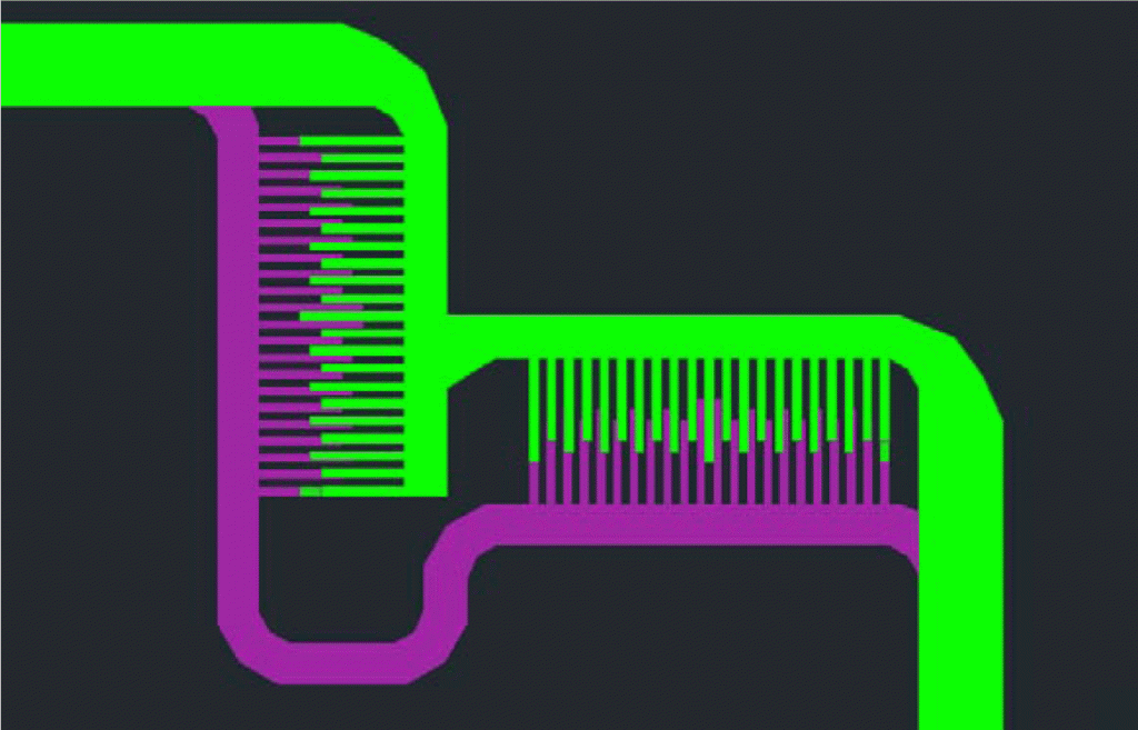
The Alignment Marker:
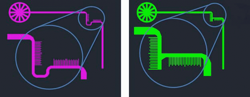
While any alignment marker can be used between layers, we suggest using the one shown in Figure 1.  The teeth act as Vernier scales in the x and y directions, thus, the degree of misalignment can be measured.  This alignment marker was designed with 10 µm wide teeth.  On the first layer (Figure 1, left), there are 22 posts which are 10 µm apart.  On the second layer, there are 20 posts each 11µm apart (Figure 1, right), making both markers 430µm wide.  The interlocking geometry of the markers is shown in Figure 2.  An inlet must be placed on the first layer’s alignment marker so that ink may flow through and stain the glass.

How do I do it?


1. Incorporate alignment marker

  • Add the alignment markers into the device design. On the silicon master that will be used to cast PDMS molds, The the channel height of the alignment marker on the silicon wafer should be in the 5 – 200 µm range.  The PDMS channel height only needs to be tall enough for Sharpie™ ink to flow through.

Figure 1. Alignment markers. The figure on the left is the alignment marker of the first level and the figure on the right is the alignment marker for the second layer.
Figure 2. Alignment markers interlocked.

2. Sharpie™ Ink Extraction

  • Put a needle onto a 1 mL – 10 mL syringe.
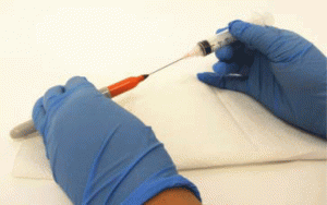
  • Insert the needle into the felt tip of a Sharpie™ marker, and slowly pull the plunger.  Slow extraction is necessary to allow air to diffuse into the marker as the ink escapes into the syringe.  Repeat as necessary.  (Figure 3)
  • Dispense the Sharpie™ ink into a microcentrifuge tube.  Sharpie™ extraction should result in 0.5 – 1 mL of Sharpie™ ink.
  • Dilute Sharpie™ ink 3X in 100% ethanol.

Figure 3. Sharpie™ extraction technique, pierce tip of Sharpie™ maker with syringe needle and slowly pull plunger.

3. First Layer

  • Cut and punch desired PDMS device.
  • Clean a glass slide and the device with Scotch™ tape.
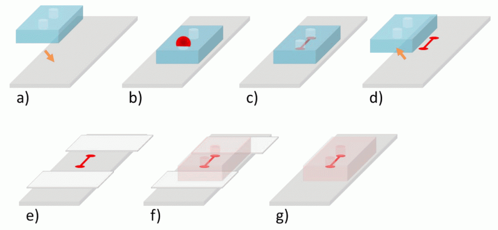
  • Reversibly bond the PDMS device onto a glass slide, by simply placing the cleaned PDMS onto the glass slide. (Figure 4a)
  • Load the Sharpie™ ink into the alignment marker channel.  This can be done by placing the device into a vacuum chamber for 5-10 minutes, removing the device from the vacuum, and placing a ~5 µL drop of Sharpie™ ink over the punch hole.  Only punch one entry hole for this method. (Figure 4b)
  • Allow the Sharpie™ ink to dry for 2 hours. (Figure 4c)
  • Remove PDMS. (Figure 4d)

Figure 4. Alignment technique schematic. a) place clean PDMS device on glass slide, b) load Sharpie™ ink, c) allow Sharpie™ ink to dry, d) remove PDMS device, e) place two pieces of scotch tape surrounding design, f) align second device to Sharpie™ ink alignment marker, g) remove scotch tape.

4. Second Layer

  • Cut and punch desired PDMS device.
  • Clean device with Scotch™ tape.
  • Place Scotch™ tape onto glass slide a few millimeters away from previous design.  (Figure 4e)
  • Under 4X or 10X magnification, bring the Sharpie™ alignment marker into the center of view and focus slightly above it.
  • Carefully place the cleaned second layer onto the scotch tape, but do not press down on the device so that the PDMS device is not in contact with the glass slide.
  • Still under the microscope, align the second layer with the Sharpie™ alignment marker by gently pushing the device along the Scotch™ tape.  The Scotch™ tape prevents the device from bonding with the glass slide.  (Figure 4f)
  • Attach the second layer by reversibly binding it to the glass slide by pressing down on the device.
  • Remove the scotch tape by holding the middle of the device down and pulling the scotch tape out from the edges of the PDMS device. (Figure 4g)
  • If additional layers are necessary, repeat second layer procedure.

What else should I know?


When using this technique by hand, the accuracy of the alignment between two layers can be down to 5 µm.  If a more precise alignment is necessary, a six axis alignment machine can be used.  As a proof-of-concept, we have reproduced Van Gogh’s Starry Night (Figure 5).  This design has two layers, and each layer was filled with Sharpie™ ink using vacuum loading.

Figure 5. 3 mm wide reproduction of Starry Night by Van Gough.

References


  1. Kane et al., Patterning proteins and cells using soft lithogrpahy, Biomaterials, 1999, 20, 2363-2376.
  2. Natarajan et al., Continuous-flow microfluidic printing of proteins for array-based applications including surface plasmon resonance imaging, Anal. Biochem., 2008, 373 (1), 141-146.
  3. Chiu et al., Patterned deposition of cells and proteins onto surfaces by using three-dimensional microfluidic systems, Proc. Natl. Acad. Sci. U. S. A., 2000, 97 (6), 2408 -2413.
  4. 3-Dimensional Molding for Making Microfluidic Devices, MicroDysis – Instrumentation Company with Micro- and Nano-fabrication, and Lab Automation, http://www.microdysis.com/TechMicrofab.aspx, 2010, accessed 16 April 2011.
Digg This
Reddit This
Stumble Now!
Share on Facebook
Bookmark this on Delicious
Share on LinkedIn
Bookmark this on Technorati
Post on Twitter
Google Buzz (aka. Google Reader)

Reusable magnetic connector for easy microchip interconnects

Myra Koesdjojo, Jintana Nammoonnoy and Vincent Remcho present a simple method to making reusable, quick release, magnetic-based fluidic connectors

Myra T. Koesdjojo*, Jintana Nammoonnoy, and Vincent T. Remcho

Department of Chemistry, Oregon State University, Corvallis, OR 97331
*Corresponding author: Myra T. Koesdjojo
Fax: (541) 737-2062
Email: koesdjom[at]onid.orst.edu

Why is this useful?


Microfluidic systems, also referred to lab-on-a-chip or micro total analysis systems (μTAS) have been developing at a rapid pace in the last decade and offers promising analytical tools that may transform routine chemical analysis in the future. Microfluidic devices typically require multiple interconnects.1 Consequently, reliable microfluidic interconnections have become one of the basic necessities in integrated fluidic and on-chip systems. The lack of an efficient interface or interconnect between microfluidic devices and the macroscale world has historically been a major challenge and one of the greatest limiters on acceptability and the application of μTAS into the broad world market. Clearly, there is a need for a low-cost, flexible interconnects for microfluidic devices to be successful in the long term.2 There are a variety of current products available and techniques that have been used to provide interfacing between microchannels to external devices.3-6 The most common and simplest approach is the direct integration of tubing or a syringe needle into the microchip inlet using epoxy glue. The drawback is it often leads to clogging of the microchannels and these types of interconnections are impractical to remove and are not reusable. This tip presents a simple method to making reusable quick release magnetic-based fluidic connectors. It is an alternative approach that provides a simple, cost effective universal interconnects in the microfluidic applications. The magnetic-based connectors was developed using two permanent magnets that form a compression seal against the tubing line and the surface of the microfluidic device. The magnetic connector also allow for standard tubing to be interfaced with the microchips. With this approach, interconnects can be easily assembled and reconfigured numerous times without causing damage to the microfluidic device. And since connection is established though a magnetic based approach, clogging of microchannels from adhesive or epoxy can be avoided.

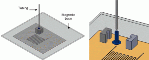
Figure 1. Picture of system components.

What do I need?


  • Permanent magnets (design and dimension shown in Figure 2)
  • Magnetic base
  • Elastic such as PDMS compression seals or vacuum cup
  • PEEK or Teflon tubing (not limited to the materials of the tubing)

What do I do?


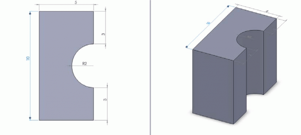
1. Custom made permanent magnet shown in Figure 2. The first component was a permanent magnet that allowed for a standard tubing to be attached to a microfluidic device via a flexible compression seal. It was manufactured with the dimensions shown below to provide a tight fitting to the flexible seal when sandwiched between two magnets, which in turns compressing the tubing inside. The magnets are Neodymium magnets which are over ten times stronger than the ceramic magnets. These magnets are ideal for use as interconnects since they provide much greater holding forces. They can be purchased from Indigo Instruments or K&J Magnetics.

Figure 2. Magnetic interconnect view from the top (left) and side (right).

2. Rubber cup compression seals The second component was a flexible rubber cup or compression seals. The dimension should be optimized so that the inner diameter of the seal should provide a tight fitting for a tubing (a in Figure 3b) and the outer diameter (b) is slightly larger than the magnets core so when it is sandwiched in between the two magnets, the tubing is tightly held. The last parameter is the diameter of the lip base (c), which should be larger than the magnet’s core so it can be compressed to the magnetic base and tightly secured against the microchip surface to prevent leaking. A variety selection of compression seal (vacuum cup) with different sizes can be purchased from McMaster-Carr.

Figure 3. Vacuum cup used as the flexible compression seal.

3. A magnetic base was used which applied pressure between the microfluidic chip and the interconnects (Figure 4). The base is particularly useful for microchip and devices having different dimensions and port locations, as the interconnects could easily be relocated.

Figure 4. Side view of a microchip and magnet interconnects setup.

4. The magnetic interconnects were placed on each of the reservoir holes of the microchip to test for leaking.

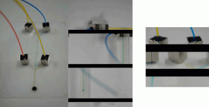
Figure 5. Setup used for a leak test (left) and a close up view of the magnetic interconnects on a chip (right).

References


[1] T. Das, D. Chakraborty and S. Chakraborty, Interfacing of microfluidic devices, Chips & Tips (Lab on a Chip), 27 February 2009.
[2] IEEE Trans. On Adv. Packaging., 2003, 26 (3), 242-247.
[3] J. Greener, W. Li, D. Voicu and E. Kumacheva, Reusable, robust NanoPort connections to PDMS chips, Chips & Tips (Lab on a Chip), 8 October 2008.
[4] http://www.upchurch.com/
[5] www.labsmith.com/microfluidicsinterconnects.html
[6] J. Micromech. Microeng., 2005, 15, 928-934.

Reusable Magnetic Connector for Easy Microchip Interconnects

Digg This
Reddit This
Stumble Now!
Share on Facebook
Bookmark this on Delicious
Share on LinkedIn
Bookmark this on Technorati
Post on Twitter
Google Buzz (aka. Google Reader)

The fabrication of PDMS interconnecting interface assisted by tubing fixation

Pengfei Li, Wei Xue and Jie Xu describe a method to connect a micro PDMS channel to peripheral microfluidic systems

Pengfei Li, Wei Xue, Jie Xu*

Mechanical Engineering, School of Engineering and Computer Science, Washington State University, Vancouver, WA 98686, USA.  E-mail: jie.xu[at]wsu.edu

Why is this useful?


Even though PDMS microfluidic devices have been widely applied in various research areas, it is still challenging to create the precise macro-to-micro interconnecting interface. Here we describe a method to connect a micro PDMS channel to the peripheral systems. With this method, we can avoid attaching exterior tubing using glue which is difficult to work with at the micro scale. In an effort to increase the connecting precision, a pre-curing step on a hot plate is adopted to prevent the tubing sliding away from the desired locations.

What do I need?


  • BD Vacutainer winged blood collection sets. (Model: 23G⨉3/4” ⨉12”, Fisher Scientific, Pittsburgh, PA, U.S.A.)
  • Dow Corning Silastic laboratory tubing. (11-189-15 Series, Fisher Scientific, Pittsburgh, PA, U.S.A.)
  • Sylgard 184 silicone elastomer kit. (Dow Corning, Midland, MI, U.S.A.)
  • SU-8 3050 permanent epoxy negative photoresist. (MicroChem, Newton, MA, U.S.A.)
  • 4-inch silicon wafer, pipette, aluminum foil, hot plate, and oven.

How do I do it?


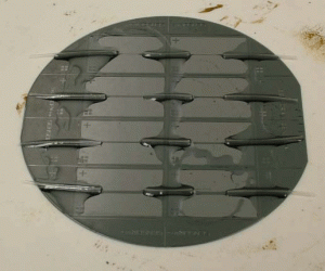
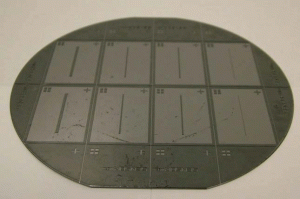
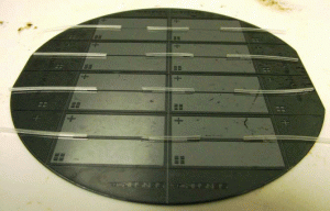
1.    Prepare the SU-8 mold on a 4-inch silicon wafer with photolithography techniques. Based on the processes from the SU-8 data sheet supplied by MicroChem, SU-8 microstructures with approximately 50 µm in thickness are fabricated for this demonstration.

2.    Mix the elastomer base and the curing agent (mass ratio 10:1) to form PDMS, remove the air bubbles thoroughly using a desiccator or a centrifuge [1].

3.    Place the silicon wafer with the SU-8 channel molds on a hot plate. The temperate is set as 60oC under which the PDMS is able to cure in 10~20 minutes.

4.    Cut the Silastic tubing into short pieces with proper length. Align the tubing section with the channel molds.

5.    Apply a small amount of PDMS to fix the tubing sections. Due to the relative high temperature of 60oC, the PDMS is nearly cured in 10~20 minutes. This step ensures that the tubing sections stay in the intended places where they are well aligned with channel molds. The tubing is still filled with air, though both ends of the tubing are sealed by PDMS.

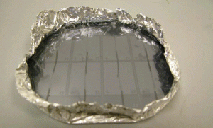
6.    Use aluminum foil to wrap the silicon wafer and create a container for storing PDMS. Extra PDMS is then quickly poured into the container and later cured in an oven [2].

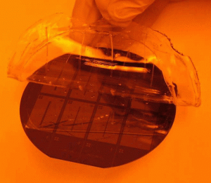
7.    Peel the cured PDMS off the channel molds and cut the PDMS into channel devices.

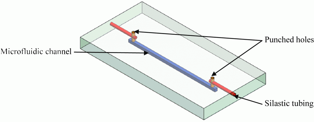
8.    Punch a small hole on each end of the channel. The tubing sections can be connected to the channels through the holes.

9.    Bond the PDMS channel to a glass substrate. Then bond another layer of PDMS as the top cover to seal the holes.

10.    Insert needles into the tubing sections. This creates the connection for the PDMS microchannel.

References


[1]  C. N. LaFratta, Degas PDMS in two minutes, Chips & Tips (Lab on a Chip), 17 August 2010.
[2] A. O’Neill, J. Soo Hoo and G. Walker, Rapid curing of PDMS for microfluidic applications, Chips and Tips , 23 October 2006.

Digg This
Reddit This
Stumble Now!
Share on Facebook
Bookmark this on Delicious
Share on LinkedIn
Bookmark this on Technorati
Post on Twitter
Google Buzz (aka. Google Reader)

Degassing a PDMS mixture without a vacuum desiccator or a laboratory centrifuge and curing the PDMS chip in an ordinary kitchen oven

Aung K. Soe and Saeid Nahavandi describe a method for degassing PDMS with readily available equipment

Aung K. Soe and Professor Saeid Nahavandi
Centre for Intelligent Systems Research, Deakin University, Australia

Why is this useful?


Whitesides (2001) advocated that soft lithography can facilitate researchers to fabricate PDMS lab-on-a-chip devices with accessible and affordable resources [1]. A typical soft lithography fabrication laboratory requires master reverse molds, a PDMS pre-polymer mixer, scales for weighing, a vacuum desiccator, an oven and oxygen plasma treatment of PDMS surfaces to become hydrophilic [2].

In soft lithography, the PDMS elastomer is first mixed with the cross-linker (curing agent) in a weight ratio of 10:1. Stirring the mixture forms air bubbles. Traditional soft lithography protocols recommend using a vacuum desiccator before pouring the mixture onto the mold master. The PDMS pre-polymer is cured fully or partially inside the oven at 80 to 95 °C for 15 to 20 minutes, transforming the resin into solid silicone rubber. However, not all researchers who need to fabricate PDMS chips have all the resources stated.

LaFratta (2010) demonstrated that a laboratory centrifuge can be used to degas PDMS [3], but a desktop laboratory centrifuge (to degas) and an oven (to cure) may not be accessible or affordable to all researchers. The technique described here uses a handheld electric mixer to mix and degas the PDMS pre-polymer. An ordinary kitchen oven is used to cure the PDMS chip.

Since the food processor cannot be used for more than 3 minutes, the procedure is done in 2 sections, each lasting 2.5 minutes with 1 minute period between them. A Pyrex® petri dish is used to hold the reverse mold (master), so the dish will not deform inside the oven. The oven must be switched on and off so that the Pyrex does not crack.

What do I need?


  • SYLGARD 184 silicone elastomer base and curing agent (Dow Corning)
  • a low-cost hand-held electric mixer
  • a kitchen grill oven with sustained heating capacity at 80 °C
  • a baking cup (or a Pyrex petri dish) and polystyrene petri dishes for PDMS chip storage
  • a polished micro-machined or patterned reverse master mold that will not float on the PDMS pre-polymer
  • a scale that can work in units of grams
  • consumables: gloves, disposable cups, 2 or 4 plastic centrifuge tubes (15 ml capacity)

How do I do it?


1. Weigh the PDMS base and curing agent in the desired ratio in a disposable cup. 10:1 is the most common ratio, but any ratio can be used depending on the desired stiffness of the cured polymer.
2. Mix base and curing agent together with the stirrer attachment of the hand-held electric mixer. Pour the pre-polymer evenly into 2 or 4 centrifuge tubes. If there is not enough pre-polymer for 2 or 4 tubes, fill 1 or 3 tubes and one more tube with water for balancing. It is important to balance the attachment during spinning. Tightly seal the centrifuge tube caps.
3. Tie the tubes to the stirrer attachments of the handheld mixer. Hold the mixer in a vertical position, switch on and spin for 2.5 minutes, then stop to give the spinner a rest for 1 minute. Turn the bottles 180 degrees and spin for another 2.5 minutes until all the bubbles have escaped from the pre-polymer mixture.
4. Pour the centrifuged PDMS onto the patterned reverse master mold in the baking cup or Pyrex petri dish.
5. Put the master mold container in the oven and cure at 80°C for 10 minutes if the baking cup is used. If the Pyrex petri dishes are used, the heat must be switched on for 5 minutes then off for 5 minutes since Pyrex dishes can crack under continuous heat. Switch the heat on and off for 30 minutes.
6. Peel the PDMS slab off the master using a sharp-tipped knife and store the PDMS chip in a polystyrene dish before autoclaving or treating with oxygen plasma.

Figure 1. Weighing, mixing and stirring

Figure 2. Before spinning

Figure 3. Spinning the tubes attached to the processor

Figure 4. After spinning

Figure 5. Acrylic reverse mold in the baking cup

Figure 6. Baking cup in ordinary kitchen oven at 80 °C

Figure 7. Peeling off PDMS slab from the baking cup

Figure 8. Storing the PDMS chip inside a petri dish


What else should I know?


The reverse master can be fabricated in microfluidics fabrication foundries at Stanford University or California Institute of Technology. Reverse masters can also be made by machining pcrylic (also known as PMMA and plexiglass) with subtractive CNC machines such as the Roland DG MDX 40. Three-dimensional additive printers can also be used. Third-party service companies can also do micro-machining and surface polishing if one wishes to outsource the master fabrication task.

References


[1] G. Whitesides et al., Soft lithography in biology and biochemistry, Annu. Rev. Biomed. Eng., 2001, 3(1), 335-373.
[2] A. Harsch et al., Pulsed plasma deposition of allylamine on polysiloxane: a stable surface for neuronal cell adhesion, J. Neurosci. Methods, 2000, 98(2), 135-144.
[3] C. N. LaFratta, Degas PDMS in two minutes, Chips & Tips (Lab on a Chip), 17 August 2010.

Digg This
Reddit This
Stumble Now!
Share on Facebook
Bookmark this on Delicious
Share on LinkedIn
Bookmark this on Technorati
Post on Twitter
Google Buzz (aka. Google Reader)