David Caballero1,2, Josep Samitier1,2
1 Nanobioengineering group, Institute for Bioengineering of Catalonia (IBEC), Barcelona, Spain
2 Centro de Investigación Biomédica en Red de Bioingeniería, Biomateriales y Nanomedicina (CIBER-BBN), Zaragoza, Spain.
Why is this useful?
Long-term imaging of cells is typically performed using standard Petri dishes. Frequently, these ´chambers´ are not convenient when sample manipulation and treatment (e.g. functionalization, immunostaining…) is needed, both before and after the experiment1. To overcome this ´problem´, glass coverslips are used. They can be easily manipulated when following multistep protocols prior to cell deposition. For live-cell microscope imaging, the customized coverslips are secured into holders (chambers) containing the adequate cell culture medium2, 3. These holders are either supplied by the microscope manufacturers or fabricated in a mechanical workshop; this implies time for the design and money.
In this work we show two different strategies for the simple, fast and cheap fabrication of chambers for live-cell imaging, using materials and simple tools typically available in a bioengineering laboratory. These materials include Petri dishes, polydymethylsiloxane (PDMS), Falcon tube cap and glass coverslips. In the first strategy (A) we drill a hole in a Petri dish where a customized glass coverslip is adhered at the bottom using wax. In the second strategy (B), a PDMS frame is used to hold the coverslip inside a Petri dish. Depending on the user final application one strategy is recommended over the other (see below). All the material is biocompatible and simple to obtain. These two methods provide several advantages: (i) they are easy and cheap; (ii) the chambers can be fabricated in a short-time period; (iii) this approach avoids the purchase of commercially-available holders or ordering the fabrication to a mechanical workshop.
What do I need?
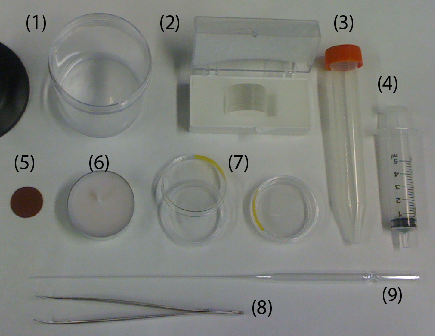
Figure 1
Figure 1. Material needed for the fabrication of the home-made chambers.
(1) PDMS
(2) Glass coverslip #1, 25 mm in diameter
(3) Cap of a 15 mL Falcon (any brand)
(4) Syringe 5mL
(5) Polishing paper
(6) Wax
(7) P35 plastic Petri dish (any brand)
(8) Sharp Tweezers
(9)Glass Pasteur pipette
You will also need:
- Hot plate
- Bunsen burner (optional)
- Soldering iron (or drill)
- EtOH 70%
- Oven
- SYLGARD 184 PDMS and crosslinker agent (Dow Corning)
What do I do?
Figure 1 (above) shows all the material needed for the fabrication of the home-made chambers using both strategies A and B. The steps describing both strategies are detailed next.
STRATEGY A:
1. Make a circular hole of around 2 cm in diameter in the middle of the lower part of a P35 Petri dish using a pre-heated, sharp-tip soldering iron. Alternatively, a drill can be used. Ensure a perfect circular hole by using a 15 mL Falcon cap as a template (see Fig.2a-c).

Figure 2. Fabrication of the cell culture chamber using Strategy A. Drilling a hole on the lower part of a Petri. (a) First, draw a circumference of about 2 cm in diameter in the center of the lower part of a Petri dish. Use a 15 mL Falcon cap as template. (b-c) Next, a soldering iron is used to drill a hole. (d) Finally, the edge of the hole is polished using thin polishing paper.
2. Polish the hole using polishing paper (see Fig.2d). Check that the Petri is free of debris. Rinse the sample with etOH 70%. (Optional: Sonicate).
3. Use the tweezers to place and secure the glass coverslip on the back side of the holey dish with its customized side (e.g. functionalized) facing the inner part of the Petri (see Fig.3a-b).

Figure 3. Adhering the glass coverslip to the lower part of the drilled Petri dish using wax. (a) The drilled Petri dish and glass coverslip #1, 25 mm in diameter are (b) placed together and secured using the tweezers. (c) Next, the wax is melted using a heat plate. A small volume is absorbed by capillarity using a glass Pasteur pipette. (d) Following the edge defined by the coverslip and the dish, the chamber is sealed. This step is critical to ensure a good sealing. (e) Check that no open remaining points are left. (f) A Bunsen burner or equivalent can be used to melt the solidified wax inside the pipette.
4. Melt the wax using the hot plate and fill the Pasteur pipette with a small volume (see Fig.3c). NOTE: Capillarity will make the liquid wax to flow inside the pipette.
5. Gently, put in contact the tip of the pipette (filled with wax) with the coverslip. Follow the edge formed by the coverslip and the Petri (see Fig.3d). Cover it completely with wax until the entire contour is sealed (see Fig.3e). Refill the pipette if necessary. NOTE 1: The wax may solidify inside the pipette quickly. If so, melt it again using the Bunsen burner (or equivalent) (see Fig.3f). NOTE 2: Ensure that no empty spaces are left; cell medium will flow through them.
6. Culture the cells of interest (see Fig.4). Place the chamber inside the microscope and start the live-cell imaging experiment. NOTE: Manipulate gently the sample.

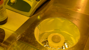
Figure 4. Finished chamber for live-cell imaging experiments. (a) Front view of the chamber filled with cell culture medium. (b) Back side view showing the wax-sealed region. No leakage is observed. The coverslip can be easily recovered after the experiment by pushing it down gently with the tweezers.
7. At the end of the experiment, the medium can be removed and the coverslip detached by pushing it down gently with the tweezers. Treat the sample as desired (e.g. immunostaining).
STRATEGY B:
1. Insert upside down the cap of a 15 mL Falcon in the middle of a P35 Petri dish (see Fig.5a).

Figure 5. Fabrication of the cell culture chamber using Strategy B. (a) A 15 mL Falcon cap is placed in the center of a P35 Petri dish. The empty region is filled with PDMS using a syringe. (b) The sample is degassed and cured. (c) The cap is removed and the PDMS frame released.
2. Fill the empty space with a syringe (or equivalent) with PDMS in a 10:1 ratio (pre-polymer:cross-linker). Degass and cure it at 65ºC for 4h (see Fig. 5b). NOTE 1: Holding the cap with adhesive tape will ensure that it remains in the center during curing. In this case, curing must be performed at RT overnight. NOTE 2: A very thin PDMS layer may appear after the removal of the cap. Remove it manually to ensure a through-hole in the PDMS. Alternatively, a weight can be applied on top of the cap.
3. Remove the cap using the tweezers and release the PDMS frame (see Fig. 5c).
4. Sterilize the PDMS frame. Rinse it with etOH 70% and UV-irradiate for 15 min.
5. Working in the cell culture room, deposit a drop (~50 uL) of culture medium in the center of a new P35 Petri dish (see Fig. 6a).

Figure 6. Finished chamber for live-cell imaging experiments. (a) A small drop of cell culture medium is deposited in the center of a new P35 Petri dish. (b) The customized coverslip is placed on top of it. (c) The PDMS frame is introduced inside the Petri and pushed down to hold the coverslip forming the chamber. Finally, the chamber is filled with cells.
6. Place the (customized) glass coverslip facing-up on top of the drop (see Fig. 6b). NOTE: This will ensure that no air bubbles are formed. Hold it with the PDMS frame.
7. Culture the cells of interest (see Fig. 6c). Place the sample inside the microscope and start the experiment.
8. At the end of the experiment, the medium can be removed and the coverslip released by removing the PDMS frame with the tweezers. Treat the sample as desired (e.g. immunostaining).

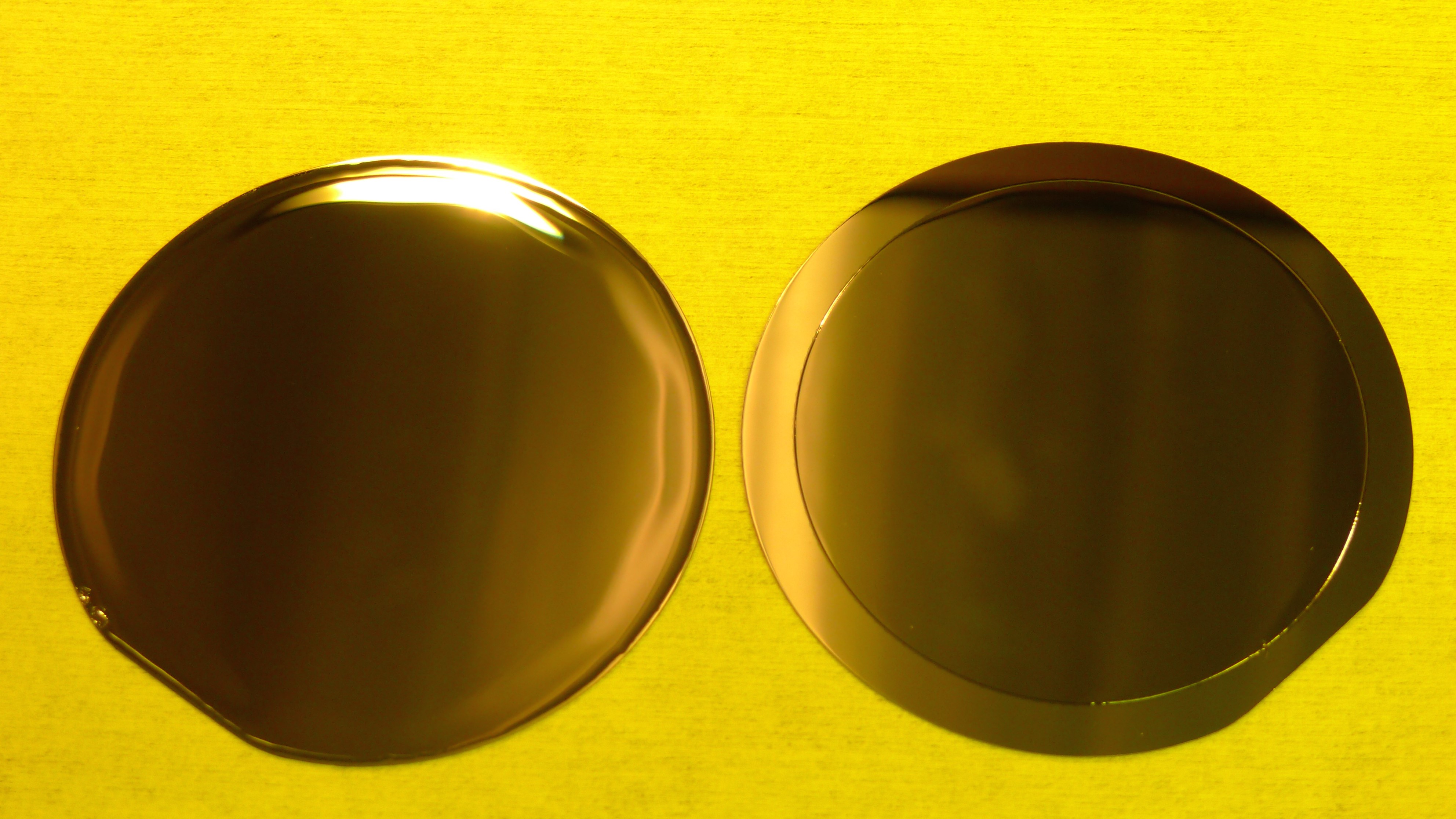
Figure 7. Microfabricated coverslips for live-cell imaging studies. (a) Glass coverslip covered with PDMS microstructures. (b) The modified coverslip can be used for the fabrication of chambers using both strategies. (c) Zoomed image of the microstructures (parallel grooves). The dimensions are: 1 um x 1 um x 1 cm (HxWxL); the separation between grooves is 1 um. Scale bar: 10 um. (d) NIH3T3 fibroblasts aligned parallel to the grooves. The arrow shows the direction of the structures. Scale bar: 50 um.
What else should I know?
By using these two approaches, chambers can be easily fabricated in the lab. Most importantly, this approach allows the manipulation of coverslips before and after the experiment with cells. If the coverslips are (bio)chemically modified (e.g. micropatterned with proteins of the extracellular matrix), manipulation must be performed carefully and fast to avoid sample degradation. Similarly, for cell guidance assays, coverslips can be easily modified with microfabricated structures to orient cell growth and motility (see Fig. 7), following the same steps described in this protocol.
For Strategy A, users must be aware of the melting temperature of wax (around 45ºC). This implies that the sealing may be fragile when performing the experiments at 37ºC and manipulation must be performed gently to avoid liquid leakage. Other materials and shapes, besides circular glass coverslips, could be used. This will depend on the experimental requirements of the user. For Strategy B, the PDMS frame and the coverslip could be used without the Petri in some applications. However, for live-cell imaging, a perfect fit between the chamber and the microscope stage is needed and the use of the Petri is therefore strongly recommended.
Finally, the user must consider the magnification needed for the experiment and the thickness of the sample on each strategy. Strategy A is recommended for high magnification microscopy (40X – 100X) and Strategy B for low magnification (4X – 20X). If needed, thinner coverslips (#0) could be used.
Acknowledgements
Dr. Daniel Riveline, Dr. Jordi Comelles (Laboratory of Cell Physics ISIS/IGBMC, Strasbourg, France) and David Izquierdo (Nanobioengineering group – IBEC, Barcelona, Spain) are acknowledged for technical help and discussions.
References
1. Zanella F, Lorens JB, Link W. High content screening: seeing is believing. Trends Biotech 2010; 28:237-45.
2. Caballero D, Voituriez R, Riveline D. Protrusion Fluctuations Direct Cell Motion. Biophysical Journal 2014; 107:34-42.
3. Riveline D, Buguin A. Devices and methods for observing the cell division WO/2010/092116, 2009.
Comments Off on Different strategies for the fabrication of cell culture chambers for live-cell imaging studies


")


 Demonstration of solder strength b) small electrode stripping as observed when the solder is removed by a strong tug")


 and the other just has to be covered with a thin polymer layer")


