Frank Benesch-Lee, Jose M. Lazaro Guevara, and Dirk R. Albrecht
Worcester Polytechnic Institute, Worcester, MA 01609 USA
Why is it useful?
Modern microfluidic devices can incorporate channels of different heights to fulfill their designed function. Examples include hydrodynamic focusing [1], cell traps [2], and chambers that isolate cellular components [3]. These devices are fabricated from a multilayer SU-8 photoresist master mold. Each layer height requires a separate set of photolithographic steps, including photoresist spin, photomask alignment, exposure, and bakes, followed by a development step at the end to reveal the 3D resist pattern.
Mask aligners have microscopes and stage micrometers for precise, micron-scale alignment of each layer’s photomask with visible marks on the substrate wafer. They are indispensable tools for creating multilayer patterns with accurate registration, but while available in cleanrooms at many research universities, their substantial expense may place them out of reach of teaching institutions and individual laboratories.
In contrast, single-layer microfluidics can be prepared using an inexpensive UV light source, or even a self-made one [4]. In principle, manual photomask alignment could be made under a microscope, then brought to the UV source, yet this poses several complications. First, alignment features can be very difficult to see using inexpensive microscopes or stereoscopes, especially in thin SU8 layers, due to poor contrast between exposed and unexposed regions before development. Second, misalignment can occur during movement to the exposure system.
Here we present a manual photomask positioning method that yields a 50 µm accuracy, without the aid of a mask aligner.
What do I need?
- Equipment and supplies for photolithography:
- Spin coater, and UV exposure system
- Substrate wafer and SU-8 photoresist
- Small microscope (e.g. USB) or stereo microscope
- Photomask transparencies for each layer
- Scotch tape
- Fine-tip permanent marker
- Straight razor blade
- Cutting mat
- 4 small (3/4”) or mini (1/2”) binder clips
- Glass plate, approx. 4 x 5”, compatible with exposure system
What do I do?
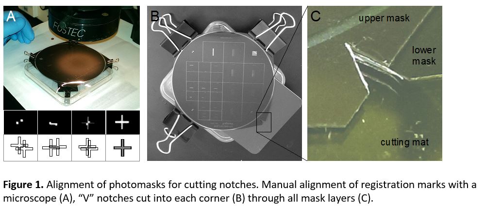
- Cut the photomasks from the transparency sheet, leaving 4 corner tabs. Align the two masks relative to each other under the microscope (Figure 1a) and clip them together with a binder clip. Ensure correct mask orientation and check alignment accuracy at multiple alignment marks across the mask. (Note that horizontal alignment accuracy with a stereomicroscope is low, because each eye’s optical path is angled 5 – 8 degrees, whereas vertical alignment is unaffected. Align in the vertical direction first then rotate the masks 90 degrees to ensure accurate alignment in both horizontal and vertical directions.) Add binder clips to each corner (Figure 1b), and verify alignment. Next, remove one binder clip at a time and use a straight razor blade to cut a sharp V-notch into each tab, through both masks. Press the blade straight down to avoid shifting the alignment. Replace the binder clip, and proceed to the next corner until all 4 notches are cut (Figure 1c).
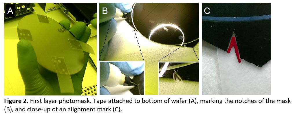
- Spin the first layer of SU-8 onto the wafer to the desired thickness and prebake. Attach 4 pieces of scotch tape onto the bottom of the wafer so that the sticky side faces up (Figure 2a). Position the first mask on the wafer, pressing gently to adhere it to the tape tabs. Use a fine-tip marker to trace the alignment notches (Figure 2b) onto the scotch tape (Figure 2c). Transfer to the UV exposure system and expose. Carefully remove the mask without detaching the scotch tape from the wafer and postbake. Scotch tape is compatible with 95 °C baking. Apply an additional piece of tape to cover the sticky tape tabs to protect the marker from smearing and allow smooth alignment of the next mask.
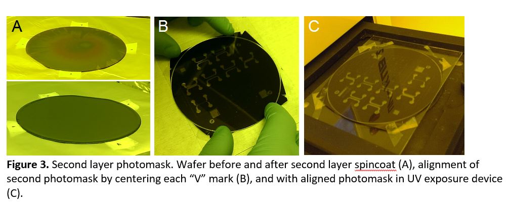
- Spin coat the next photoresist layer and prebake (Figure 3a). Mount the wafer onto a glass plate with a loop of scotch tape to keep it in place. Position the second mask onto the wafer, ensuring that alignment “V” markings are centered within each alignment notch and across all 4 corners (Figure 3b). Affix the mask to the glass plate with thin (2-3 mm wide) pieces of tape, and adjust alignment as necessary. Carefully transfer the glass plate with wafer and aligned photomask for exposure (Figure 3c).
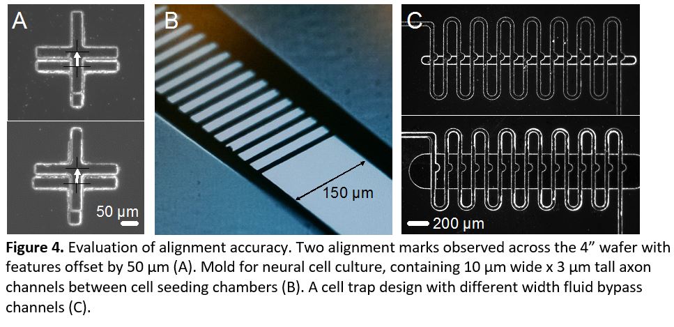
- Repeat step 3 for any additional layers. Remove the tape tabs and develop the photoresist. Evaluate alignment accuracy under a microscope (Figure 4).
Conclusions:
In this tip, we present a method for manual alignment of multiple transparency photomasks. We achieved repeatable accuracy of <100 µm and as good as 50 µm (Figure 4a). These accuracies are within required tolerances of many multilayer designs (Figure 4b). In many cases, minor design alternatives can relax alignment tolerances, such as in a trap design containing a thin horizontal channel that allows fluid bypass but captures larger objects (Figure 4c). In this example, a 100 µm wide bypass channel only partially covered the trap indentations, whereas widening the bypass channel to 400 µm enabled a functional device despite slight misalignment. Overall, this simple method allows fabrication of microfluidic device molds containing multiple layer heights, without expensive mask alignment equipment, to an accuracy of at least 50 µm. Furthermore, after alignment marks are cut, no microscope is needed at all during the photolithography process, speeding the fabrication of multiple masters.
Acknowledgments:
Funding provided by NSF IGERT DGE 1144804 (FBL), Fulbright LASPAU (JMLG), University of San Carlos of Guatemala (JMLG), NSF CBET 1605679 (DRA), NIH R01DC016058 (DRA), and Burroughs Wellcome CASI (DRA).Acknowledgments:
References:
- Chih-Chang, C., H. Zhi-Xiong, and Y. Ruey-Jen, Three-dimensional hydrodynamic focusing in two-layer polydimethylsiloxane (PDMS) microchannels. Journal of Micromechanics and Microengineering, 2007. 17(8): p. 1479.
- Erickson, J., et al., Caged neuron MEA: A system for long-term investigation of cultured neural network connectivity. Journal of Neuroscience Methods, 2008. 175(1): p. 1-16.
- Taylor, A. M., et al., A microfluidic culture platform for CNS axonal injury, regeneration and transport. Nature Methods, 2005. 2(8): p. 599-605.
- Erickstad, M., E. Gutierrez, and A. Groisman, A low-cost low-maintenance ultraviolet lithography light source based on light-emitting diodes. Lab on a Chip, 2015. 15(1): p. 57-61.


")