It allows to remove and bind different PDMS structures many times to one and the same glass surface. It is especially useful for electrochemical measurements where the glass surface is coated with metal electrodes [1,2]. It allows to test different channel geometries on one and the same electrodes which saves money and time required for depositing new electrodes.
What problem does it solve?
If the channel is clogged, damaged or simply we want to do electrochemistry with different channel geometry, we do not have to make new electrodes on glass. We can remove the unwanted PDMS structure and re-use the glass plate with the new channels.
What do I need?
Concentrated H2SO4, glass pipette, glass beaker, tweezers, gloves and lab glasses to work with concentrated H2SO4.
What do I do?
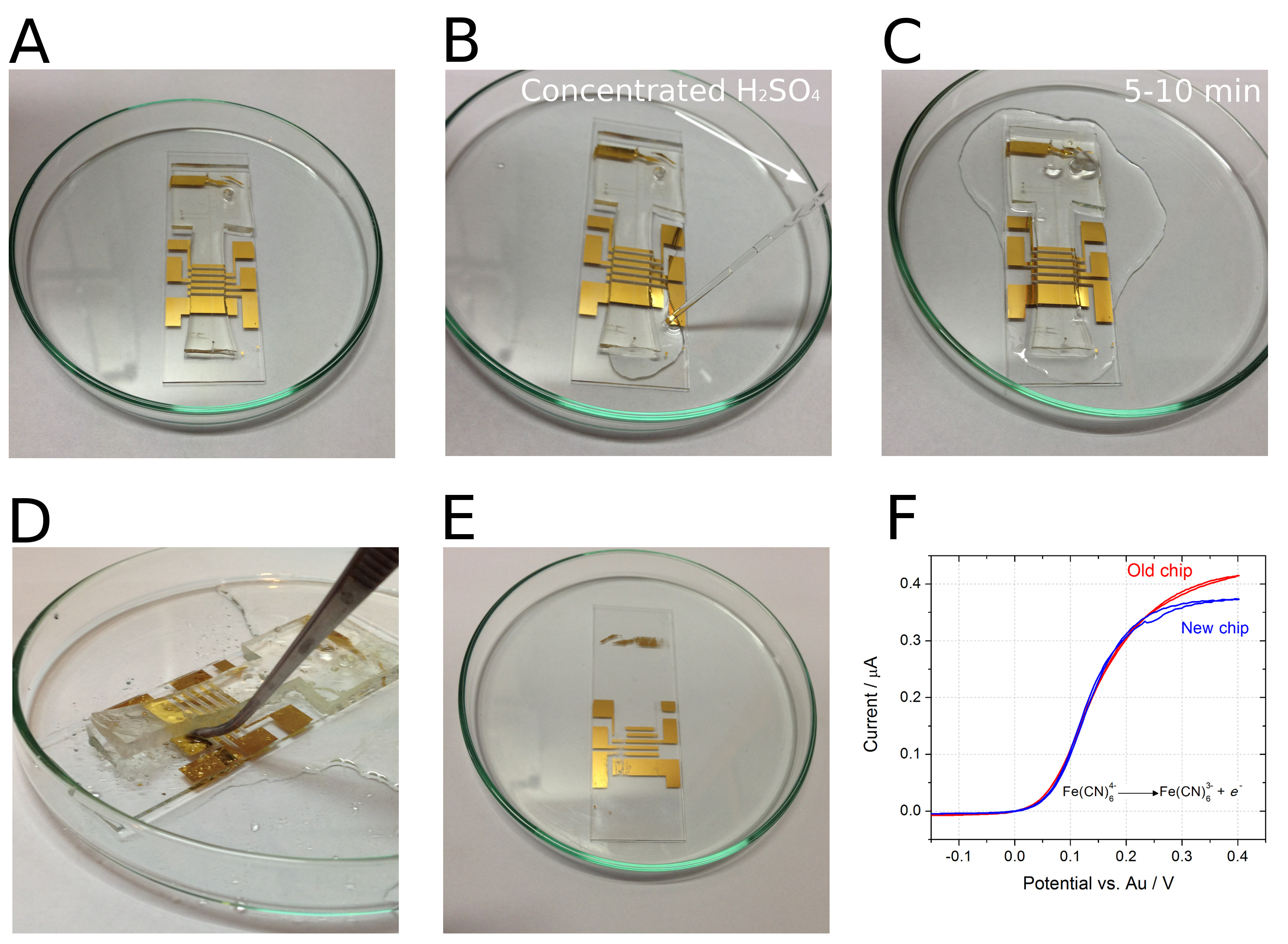
Put the PDMS chip in a Petri dish (Figure A).
With a glass pipette, add concentrated H2SO4 along the edges of PDMS (Figure B).
Leave the chip in contact with H2SO4 for a few minutes.
Gently peel off PDMS from the glass using tweezers (Figure D).
Wash the glass plate with water.
The glass plate is ready for plasma-binding to a new PDMS structure.
References
[1] D. Kaluza, W. Adamiak, T. Kalwarczyk, K. Sozanski, M. Opallo, M. Jönsson-Niedziolka, Langmuir2013, 29, 16034-16039.
[2] D. Kaluza, W. Adamiak, M. Opallo, M. Jönsson-Niedziolka, Electrochim. Acta2014, 132, 158-164.
Comments Off on How to remove plasma-bonded PDMS from glass?
Sukru U Senveli, Rajapaksha WRL Gajasinghe, and Onur Tigli
Department of Electrical and Computer Engineering, University of Miami, Coral Gables, FL, USA and
Biomedical Nanotechnology Institute at University of Miami (BioNIUM), Miami, FL, USA
Why is this useful?
PDMS (Polydimethylsiloxane) is a widely used material for fabricating microchannels through molding processes. In some studies, the exact position or dimensions of the PDMS microchannel on an active substrate is not very important, especially if no active manipulation or sensing is desired with microfluidics. However, there are many studies that can benefit from precise aligning of microchannels to structures on a substrate for optimum system performance. In such cases, coarse alignment using only tweezers may not be an option as overlay accuracy is limited to around millimeter scale. Plasma activated PDMS is a good example of this case where irreversible bonding requires bonding with one try in a short amount of time. Furthermore, there are cases in which the outer dimensions of the PDMS slab become important where cutting the PDMS using razors alone is not precise enough. Possible reasons for needing well-defined outlines include housing requirements and necessity of electrical access.
This study deals with methods to
fabricate microchannels with well-defined shapes using a plastic template on a handle substrate and
align and bond these microchannels onto an active substrate with high precision.
The error in outline dimensions of the microchannels was seen to be approximately 100 µm but it is ultimately limited by the 3D-printer’s accuracy. On the other hand, the overlay error was measured to be as small as <10 µm in our experiments.
We demonstrate the method on bonding of microchannels to surface acoustic wave devices on a lithium niobate substrate. The microchannel and the sidewalls need to be in the center of the region between the two devices facing each other whereas the electrical pads should be accessible and not covered with PDMS.
What do I need?
3D-printer with ABS filament
3D-printed microchannel template
3D-printed alignment apparatus
Probe station with microscope
Silicon wafer with SU-8 patterns for molding
Tri-chloro-silane (#175552 Sigma Aldrich)
Vacuum desiccator (Bel-Art)
PDMS kit (Sylgard 184)
Microscope slides
Razors
Large binder clips
3M Scotch tape
Tweezers with blunt tips
Biopsy punch
Neodymium magnets
Pipettes
What do I do?
Microchannel Fabrication with 3D-Printed Template
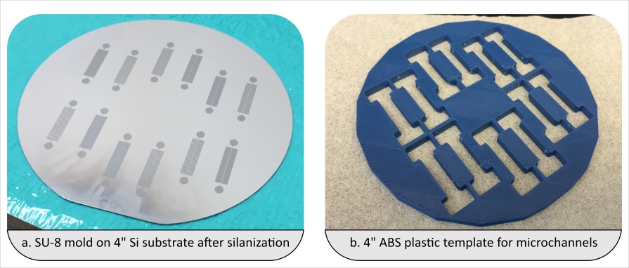
1. It is assumed that SU-8 patterns are already formed on a silicon wafer as shown in Fig. 1(a). A template mask is designed with a CAD program and fabricated using a 3D-printer with ABS type plastic to define the outline of the microchannels. A template thickness of at least 3 mm is recommended for durable microchannels and less than 6 mm is recommended for ease of punching. Fig. 1(b) shows the template structure made of ABS.
2. Under a chemical fume hood, one drop of tri-chloro-silane is placed on a microscope slide, which is in turn placed in a small vacuum chamber. The silicon wafer with SU-8 microchannel patterns is placed inside alongside the microscope slide. The chamber is closed and pumped down. After pumping down for 5 minutes to -0.8 atm of relative vacuum, the chamber is left for 2 hours for silane deposition on the silicon surface. Silane formation is visually checked after the prescribed duration as shown in Fig. 1(a).
Fig. 1 (a) Silanized mold with SU-8 features of the microchannels. (b) The 3D-printed template for microchannel outlines.
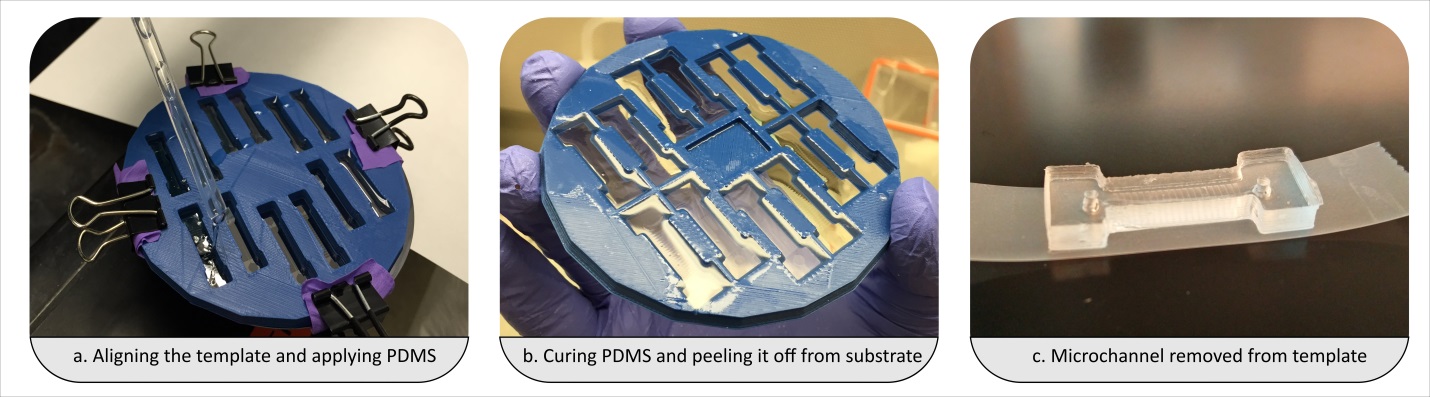
3. The 3D-printed template is carefully aligned to the substrate and held in place using paperclips. PDMS (Sylgard) mixed at a ratio of 10:1 is poured onto the holes in the filter. The amount of PDMS leaking between the filter and the substrate should be kept to a minimum.
4. A razor or another flat and sharp object is used to sweep off the excess PDMS from the top. This makes it easier in the eventual alignment step using the microscope. The assembly with the plastic template in place on the substrate and filled with PDMS is shown in Fig. 2(a). Binder clips are used to hold them close together.
5. PDMS is left to cure overnight.
6. The template is separated from the substrate by first cutting through the interface with a razor from the sides and then wedging in with tweezers from four different locations around the substrate. A removed template is shown in Fig. 2(b).
7. Once the template is removed, the backsides of the microchannels are immediately covered entirely with Scotch tape to avoid any dust particles on the bonding surface.
8. Individual microchannels are popped out from the filter by applying uniform pressure from the top side.
9. Inlet and outlet holes are formed using biopsy punches with appropriate gauges. An example of individual channels obtained like this is shown in Fig. 2(c).
Fig. 2 (a) Template after aligning with the substrate is held in place using binder clips. (b) Template after separation from the substrate. (c) A microchannel popped out and punched for inlet and outlet.
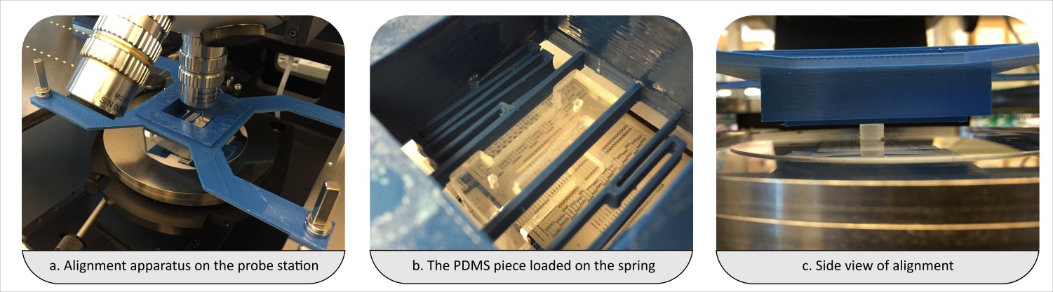
Microchannel Alignment with 3D-Printed Alignment Apparatus on a Probe Station
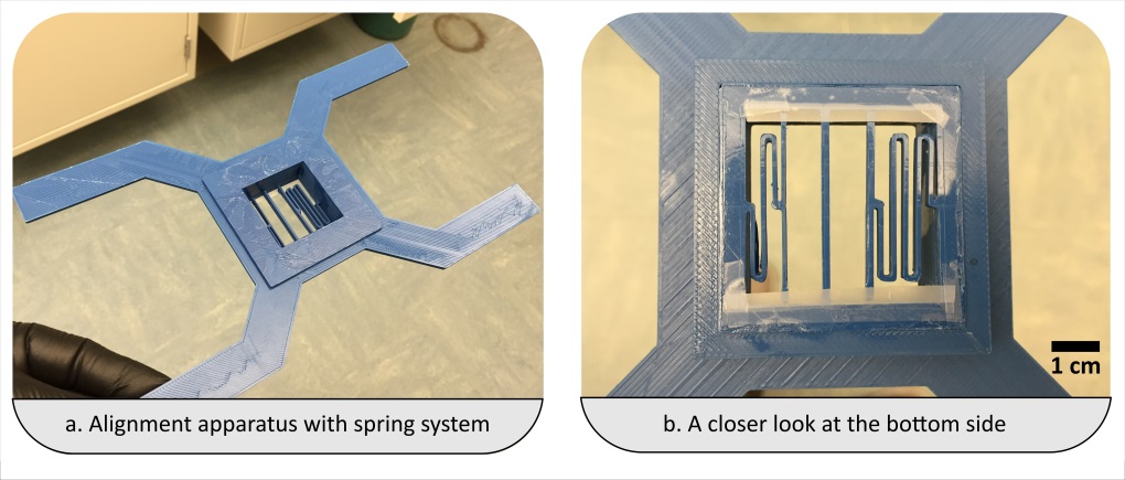
1. The microchannels are placed in the alignment apparatus shown in Fig. 3(a) between the appropriate spring and the stationary beam which are displayed in Fig. 3(b). The choice of spring depends on the spring constant and the size of the microchannel. The microchannel should be sitting flat between the spring and the beam. This can be checked by looking from the side.
Fig. 3 (a) Alignment apparatus as prototyped. (b) Bottom side of the apparatus showing the stationary beam in the middle and two springs on either side for clamping the microchannel for alignment.
2. After correct placement of the microchannel, the scotch tape can be removed slowly by shearing it in order not to disturb the PDMS piece.
3. The alignment apparatus is slowly placed on the platen of the probe station. Neodymium magnets are placed on its four legs to balance and secure the alignment piece in place as shown in Fig. 4(a). A PDMS piece loaded against the spring with a lower spring constant and the stationary beam is shown in Fig. 4(b).
Fig. 4 (a) Alignment apparatus is secured using neodymium magnets on the probe station platen. (b) A closer look at a PDMS piece loaded onto the apparatus. (c) Side view of alignment.
4. Alignment is carried out while observing the overlay using the microscope of the probe station. The overlay is controlled by the stage which moves in plane with the substrate.
5. When the alignment is made, the microchannel is lowered carefully and slowly onto the substrate to bring them into contact as shown in Fig. 4(c).
6. Blunt tipped tweezers are used to apply pressure on the top of the PDMS piece to hold it in place and for a more uniform bond.
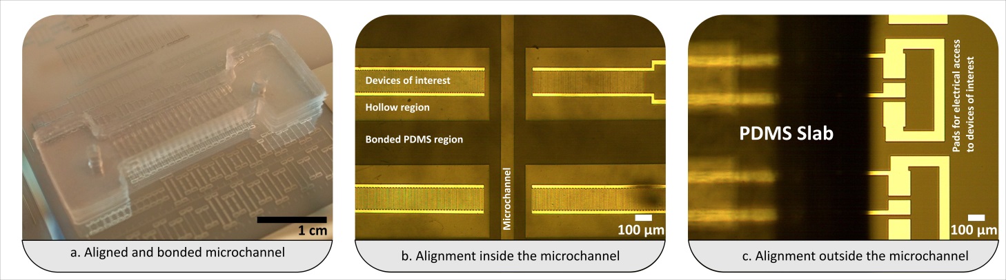
7. The spring is released with another set of tweezers. The alignment apparatus is raised by hoisting the platen without touching the sample again. The microchannel has been bonded at this step as displayed in Fig. 5 (a).
8. Microchannel alignment and bonding is double checked using the microscope as shown in Fig. 5(b-c).
Fig. 5 (a) Photograph of after successfully completed alignment and bonding. (b) Evaluation of the alignment of the microchannel to a substrate containing a set of SAW devices. The PDMS is designed in such a way as to bond on areas excluding the interdigitated electrodes of the devices marked as “Devices of interest”. The microchannel was aligned down to an alignment error of <10 µm. (c) The PDMS slab outline does not cover the pads which are available for electrical access using probes.
What else should I know?
Materials other than ABS might also be convenient for forming templates too but ABS was preferred due to its higher temperature resilience (in case a high temperature curing of PDMS is desired).
If there is a considerable amount of leakage between the template and the handle substrate, it becomes harder to separate the two. This is where the silanization helps. Also, the microchannel outlines might need to be traced using a razor in case there is a substantial amount of residue.
Overnight curing is optional. However, lower temperature/longer duration curing was seen to perform better than higher temperature/shorter duration curing step as it results in somewhat softer PDMS.
The PDMS piece sitting flat on the alignment apparatus is of utmost importance. The bottom of a 4mm tall PDMS piece should be peeking about 2 mm from the bottom of the alignment apparatus.
The Scotch tape can also be removed from PDMS before placement onto the apparatus but this can increase the chances of it collecting dust if not in a cleanroom environment.
Activation of PDMS piece and/or substrate is optional. In our studies, we did not use an oxygen plasma and the microchannel was able to withstand microfluidic operations with estimated pressure levels about -200 kPa.
Scotch tape was applied to the bottom side of the alignment apparatus to keep the springs from buckling down with the added mass from the PDMS piece.
Acknowledgment
Support from the National Science Foundation (NSF) under grant No. ECCS-1349245 is gratefully acknowledged by the authors.
Comments Off on Precise Microchannel Fabrication and Alignment with Rapid Prototyped Apparatus
Most of microfluidic devices use channels with rectangular cross-sections. The microfabrication of rectangular shaped channels is straightforward with standard tools such as photolithography.
Fluid dynamics, rheology, soft matter and, recently, biology-based investigations need circular cross-section microchannels; indeed, pre-fabricated capillaries are normally used to carry out the studies. However, capillaries are impractical for some investigations requiring complicated designs.
For Plexiglas® (or other plastic) devices, microfabrication by micromilling is a low cost procedure, which, in the last decades, has gained popularity in the field of microfluidic applications.1-2 The fabrication and the sealing of Plexiglas® microchannels with circular cross-section can be challenging.
Here, a method of fabrication of plastic microfluidic devices with circular cross-section is presented. The method is low cost and it can be performed by minimally trained users. The alignment step builds on a procedure first introduced by Lu et al. that used circular magnets to align layers of polydimethylsiloxane (PDMS).3 The protocol is validated for circular cross-section channels, but it can be used for fabricating rectangular channels or special inlets as well.
What do I need?
Plexiglas® sheets (thickness 1mm) Rohm Italy
CNC MicroMill (Minitech, US)
Ball nose end-mills (0.001 inch, PMT Endmill)
Magnets 4 mm × 4 mm× 4 mm, DX
Microscope Bresser 58-02520
Clamps RS Italy
Ethanol
Microscope (or stereomicroscope)
Glass slides for microscopy (50 mm × 75 mm)
What do I do?
1. Computer aided design of the device (CAD).
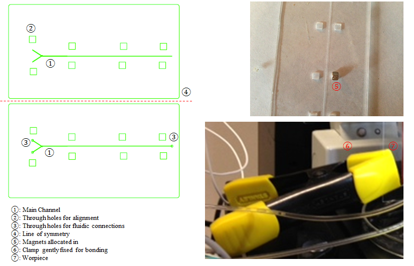
Design the microfluidic channels with CAD software. Fig. 1a displays the top and bottom layer of the main channel and, in particular, aligned square through-holes in each layer.
Translate the CAD file to Computer Numerical Control (CNC) code for micromilling.
2. Micromilling
The endmill should be aligned to set the point z=0 by using a microscope.
Then, the microchannels (top and bottom) must be milled. Channel with depends on the endmill diameter.4 It is worth emphasizing that setting the correct work parameters (such as tool speed and depth) is crucial. Indeed, if the latter are not appropriate, the plastic workpiece develops internal stresses that during the bonding result in cracks and chip breakdown.
Finally, the through holes and the frame have to be milled. The number of through holes for locating the magnets depends on the dimension of the microfluidic device. It is good practice for the rectangular through-holes to have a pitch of roughly 10 mm (this dimension depends on the size of the microchannels and of the magnets).
3. Alignment
Align the top and bottom layers with a stereomicroscope (Fig. 1b). The bottom layer should be set on a solid surface and the magnets inserted into the through-holes. Then, the second layer should be placed on the first and a second set of magnets inserted in the square through-holes of the second layer.
The magnets located in the first and second layer naturally provide a good “first alignment” of the microchannels, while leaving freedom to slightly adjust the layers (i.e., this is a reversible sealing). Once the magnets are fixed, the quality of the alignment should be checked with a microscope.
Fig. 1. The Fabrication. a. CAD design of a microfluidic channel with circular cross section. The length of the microfluidic device is 40mm, the width is 15mm. The depth of grooves is 50μm, width 25μm. b. Magnets employed for the bonding. C. Clamps used for sealing the microchannel.
4.Bonding
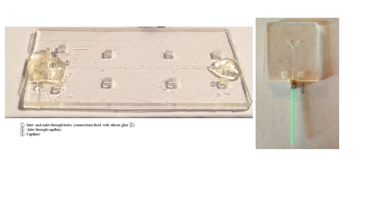
Clamp the Plexiglas® layers together and submerge assembly in ethanol for 15 minutes (Fig. 1c). For optimal bonding, the clamping should be done with clamps positioned at the edges of the Plexiglas®.5
After 15 minutes, the sealing of the microfluidic channels should be checked. If the Plexiglas® is sufficiently bonded, the magnets can be removed and glass slides placed on either side of the Plexiglas® layers. Clamp the glass slides and allow the assembly to rest for another 5-15 minutes.
The device is ready to be used for different applications as shown in Fig. 2a. Capillary tubing can be easily connected to the channel for modular design (Fig. 2b).
Fig. 2. Examples of microfluidic devices. a. Perfusion of the samples through hole at the inlet. b. Perfusion through capillaries.
In conclusion, analyzing the protocol, the following advantages can be emphasized:
The process is designed for different materials, but it fits perfectly with Plexiglas®
The equipment necessary for the fabrication and assembly includes simply a micromilling machine and a (stereo)microscope
The use of square magnets (instead of circular ones) allows for more precise alignment due to further restriction to the sliding of the top and bottom layers.
References
G. Simone, G. Perozziello, J. Nanosc. Nanotech., 2010, 11, 2057.
Hoon Suk Rho1, Yoonsun Yang2, Henk-Willem Veltkamp1, and Han Gardeniers1
1Mesoscale Chemical Systems Group, MESA+ Institute for Nanotechnology, University of Twente, The Netherlands.
2Medical Cell BioPhysics Group, MIRA Institute for Biomedical Technology and Technical Medicine, University of Twente, The Netherlands.
Why is this useful?
Most common way to handle and transport reagents in chemical or biological labs is by using a pipette. However, tubing connection is generally used for the delivery of reagents into a microfluidic device. Even though the connection with commercial tubing and connectors allows various choices on the sizes and materials of the tubing and easy connection, difficult sampling from stock solutions, dead volume in tubing and connectors, and extra sterilization on tubing and connectors for biomaterials, still remain challenges. Here we demonstrate a direct connection of pipette tips to a PDMS device and loading reagents by pressure driven flow.
What do I need?
Stainless still puncher (Syneo LLC)
Precision stainless steel tip (23 gauge, #7018302, Nordson Corporation)
Tygon tubing (0.020″ x 0.060″OD, #EW-06418-02, Cole-Parmer Instrument Company)
3D printed plug
Pliers
What do I do?
Punching inlet and outlet on a PDMS device
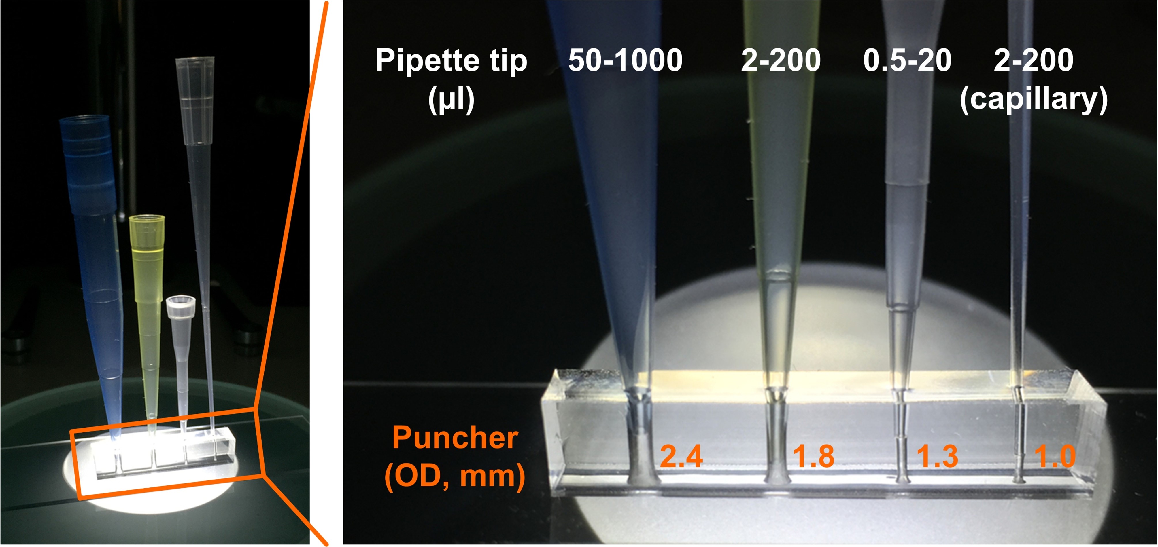
1. Select the size of a puncher based on the size of a pipette tip will be connected. We achieved tight connections of pipette tips on a PDMS substrate when we punched holes by using punchers with outer diameter of 2.4 mm, 1.8 mm, 1.3 mm, and 1.0 mm for 50 – 1000 µl, 2 – 200 µl, 0.5 – 20 µl, and 2 – 200 µl (capillary) pipette tips, respectively.
Fig. 1 Direct connection of pipette tips on a PDMS device.
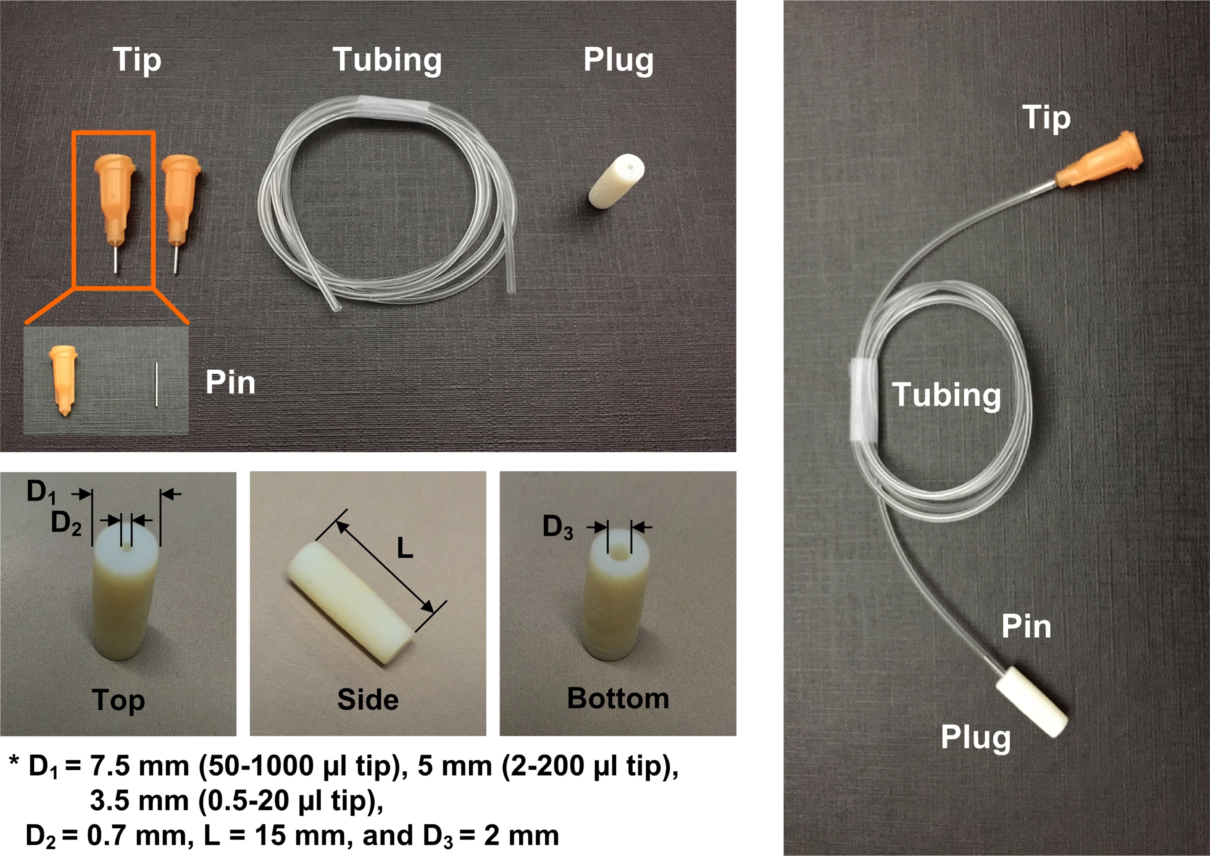
Plug connection preparation
1. Separate a pin from a precision stainless steel tip. The pin can be easily removed by twisting the plastic part while the pin is held by pliers.
2. 3D-print a plug. The outer diameter of the plug depends on the size of the pipette tip that will be connected. The detailed dimensions of the plug are shown in Fig. 2.
3. Connect a precision stainless steel tip, tubing, a pin, and a plug. Because the plastic part of the tip is luer tapped, it can be connected to male luer connectors and commercial plastic syringes.
Fig. 2 Tubing connection with a 3D-printed plug.
Solution loading
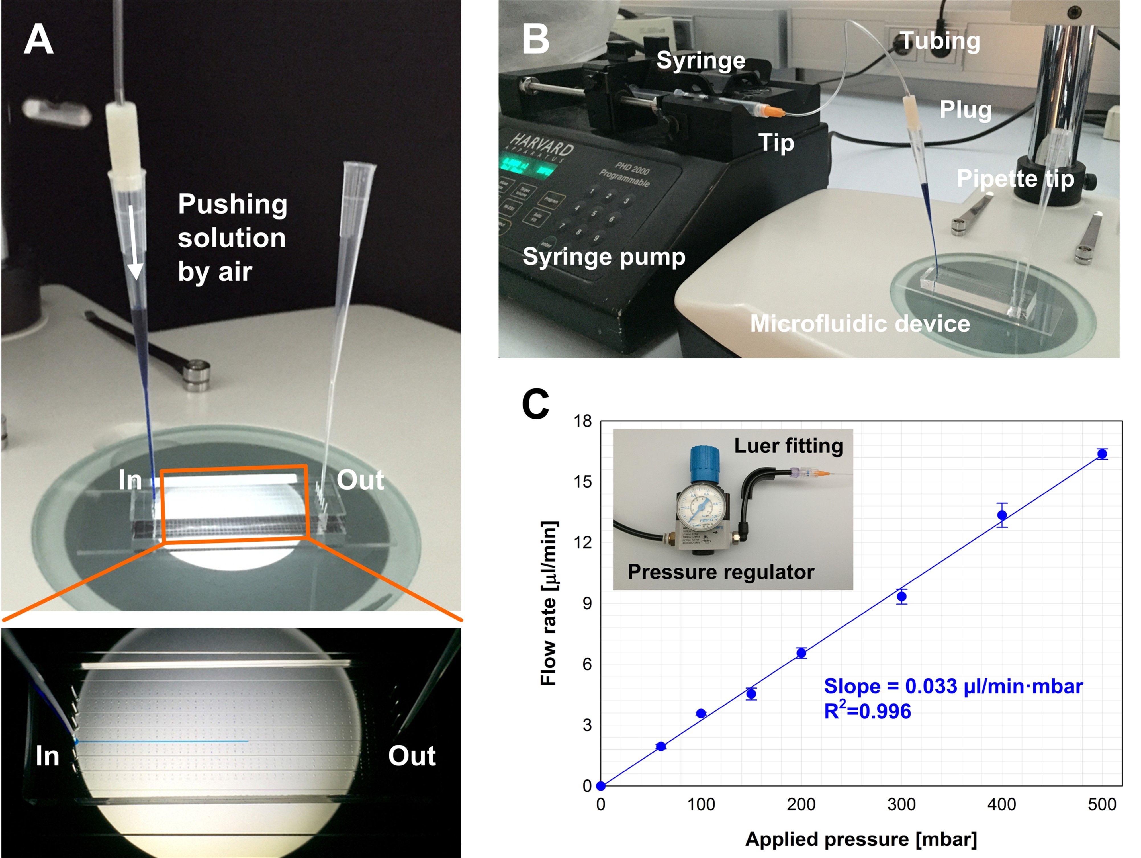
1. Pipette the sample, connect the pipette tip into the inlet of a PDMS device, and take off the pipette. When an empty pipette tip is connected into the outlet of the device, the sample from the outlet can be collected in the tip.
2. Insert the plug into the tip and connect the tip to a pressure source. When pressure is applied into the pipette tip, the solution in the tip is pushed into a microchannel (Fig. 3A). The luer tip can be connected to a syringe and a syringe pump can be used as a pressure source (Fig. 3B). The flow rate of the sample solution can be controlled by the syringe pump. The luer tip also can be connected to a pressure regulator with a luer fitting. Fig. 3C shows the flow rate of sample loading at various applied pressures controlled by a pressure regulator. In this case an external gas source is required. However, this system is cheaper than commercial microfluidic flow control systems. Also a digital pressure regulator can be used for accurate flow rate control at the low flow rate regime less than 1 µl/min.
Fig. 3 A. Loading blue food dye solution into a microchannel, B. Solution loading by a syringe pump, and C. Solution loading by using a pressure regulator.
What else should I know?
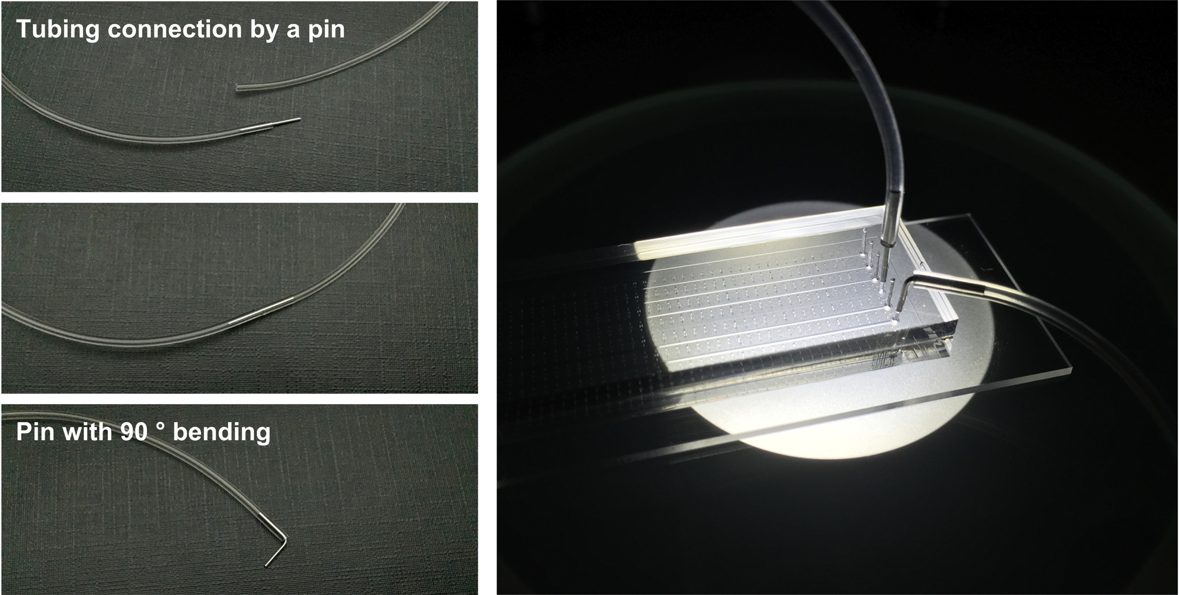
No leakage of the solution was observed in the connection of a pipette tip onto a 1mm thick PDMS substrate. However at least a thickness of 3 mm is highly recommended to achieve tight fitting and stable support for the pipette tip. The pin obtained from a precision stainless tip is very useful for tubing connections. For example two separated tubes can be connected by the pin and also the pin can be inserted into an inlet or outlet of a PDMS device punched by a puncher with an outer diameter of 1mm. Also the pin can be easily bent by using pliers for compact connection to a PDMS device.
Fig. 4 Tubing connection by using the pin from a precision stainless tip.
Comments Off on Direct Delivery of Reagents from a Pipette Tip to a PDMS Microfluidic Device
Alexander Price, Wesley Cochrane and Brian Paegel Department of Chemistry, The Scripps Research Institute, Jupiter FL 33458
Why is this useful?
Syringe pumps are the most popular tool for transporting fluids within microfluidic devices. In the process of loading sample into a syringe, air bubbles (derived from the syringe dead volume) frequently migrate into the barrel and require removal to achieve consistent flow. Ideally, a researcher would have a large excess of sample so that the barrel can be filled and evacuated multiple times. During loading, syringes are held vertically with the sample directly below the tip, necessitating forceful evacuation to dislodge rising bubbles, however this not feasible for low/intermediate-volume “precious” samples (50-500 µL). Here, we present a simple funnel to aid bubble removal during syringe loading.
What do I need?
Plastic transfer pipets (FisherBrand 13-711-7M)
Razor blade
Pipette and pipette tips
Syringe (we use Hamilton Gastight 1700 series w/ TLL tips)
What do I do?
1. Using the razor blade, carefully cut the end off of the transfer pipet so that it fits snugly over the tip of your syringe (Fig. 1). It might take a couple tries, but you can use this as a template once you have found the right location to cut.
2. Cut the transfer pipette again, roughly 2 inches up from the previous cut (Fig. 1). Your funnel is complete.
3. Attach the funnel onto the tip of the syringe. Holding the syringe vertically (funnel up), load your sample into the bottom of the funnel (Fig. 2).
4. Fill and evacuate the syringe barrel as needed to eliminate any air bubbles (Fig. 3).
5. Dispose of the funnel.
Figure 1. Construction of a syringe funnel from a transfer pipet.
Figure 2. The funnel is attached to the syringe (left), and sample is loaded into the bottom of the funnel (middle and right).
Figure 3. Air bubbles in the barrel are expelled into the funnel and syringe is filled.
Comments Off on Syringe funnels for facile loading of precious samples
David J. Guckenberger,*aJake Kanack,*aLoren Stallcop,b David J. Beebea
aDepartment of Biomedical Engineering, Wisconsin Institutes for Medical Research, University of Wisconsin-Madison, Madison, WI, USA bDepartment of Materials Science and Engineering, University of Wisconsin –Madison, Madison, WI, USA * Authors contributed equally
Why is this useful?
With several microfabrication techniques now available, including: 3D-printing,1 micromilling,2 and hot embossing,3 in-house fabrication of thermoplastic microdevices has become cheaper, faster, and easier. However, for many applications – such as cell culture and microscopy – these devices must be bonded to optically-transparent substrates such as glass. While bonding similar materials, such as Polystyrene (PS) to PS, is relatively simple, bonding dissimilar materials, such as PS to glass, presents a particular challenge. Current methods to circumvent these challenges include spin coating adhesives, such as polydimethylsiloxane (PDMS), onto sacrificial substrates4 and injecting adhesive directly into the bond interface.5 However, equipment requirements, associate long cure times, heterogeneity in glue uniformity, and complexity limit acceptance of these techniques.
Here we present simple technique for applying uniform layers of adhesive to enable rapid – less than a minute – bonding of PS to glass. Using UV-curable adhesives, readily accessible materials, and a simple techniques, we demonstrate how to apply thin uniform layers of adhesive to a microchannel. We provide design suggestions that will improve bonding repeatability, and additional information that may help apply this technique to materials beyond PS and glass.
Adhesives are often material-specific. Consult the manufacturer to determine the best adhesive for your application.
Tip: Some adhesives may require post-treatment / aging to reach a full cure.
We have tested this protocol with Ultra Light-Weld 3025 (Dymax) and Norland Optical Adhesive 68 (Thor Labs, Inc.). These adhesives had similar performance, however the protocol may need to be tailored for other adhesives.
If the adhesive is too viscous or does not adequately wick around the rib, heat may be applied to achieve thinner adhesive layers, or to improve the wicking of the adhesive.
This protocol is amenable to wide variety of materials, including: cyclic olefin copolymer (COC), glass, metal, PS, and various rapid-prototyping materials.
Creating the rib and allowing the adhesive to wick eliminates excess adhesive and prevents adhesive from squeezing into the microchannel.
What do I do?
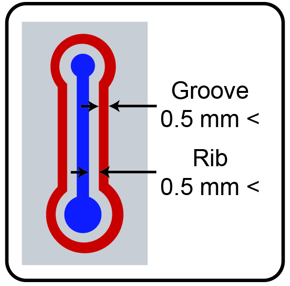
Fig.1 Channel border design
Step 1: Fabricate the microdevice. To improve bonding repeatability and adhesive distribution we recommend fabricating a groove (thickness > 0.5mm) around the channel – leaving a rib (0.5 mm < thickness < 1.5 mm) around the perimeter of the channel.
Tip: Rib thickness may need to be tuned for individual adhesives
Tip: Extra caution while applying the adhesive may be necessary for channels shallower than 0.1 mm
Step 2: Thoroughly clean the surface of the microdevice, silicone foam sheet, and coverslip using isopropyl alcohol and low-particulate wipers. Remaining particulates can be blown off with compressed air. Ensure PS and glass surfaces remain clean throughout the bonding process.
Step 3: Apply a dollop of UV curable adhesive to the foam sheet.
Step 4: Use a tongue depressor to spread the adhesive into a uniformly thin layer across the foam. The area of the adhesive should be larger than the microdevice – add more adhesive if necessary.
Step 5: Position the device onto the adhesive bonding surface down. Press down gently; avoid sliding the microdevice to prevent build-up of adhesive within the channels. Pick up the device and repeat this step two or three times to ensure the bonding surface is completely covered with adhesive.
Tip: Take care to ensure no adhesive is transferred from gloves to surfaces of the device not intended to be bonded.
Tip: Minimize the delay between step 4 and step 5 to help ensure a uniform thickness of adhesive
Step 6: Position the microdevice above the coverslip, and gently lower it until it makes contact. Once contact is made, release the device, taking extra caution to avoid sliding the microdevice.
Tip: The adhesive may have a yellow color after bonding. If necessary, allow 24 hours for adhesive to clear
Step 7: Allow a few seconds for the adhesive to wick along the ribs, then cure device for 20 seconds with ~350 nm UV light at [Intensity]
Fig. 2 Process workflow
What else should I know?
Fig. 3 Cross sectional image of a PS microchannel bonded to a glass coverslip. Scale bar represent 0.5 mm
• Adhesives are often material-specific. Consult the manufacturer to determine the best adhesive for your application.
Tip: Some adhesives may require post-treatment / aging to reach a full cure.
• We have tested this protocol with Ultra Light-Weld 3025 (Dymax) and Norland Optical Adhesive 68 (Thor Labs, Inc.). These adhesives had similar performance, however the protocol may need to be tailored for other adhesives.
• If the adhesive is too viscous or does not adequately wick around the rib, heat may be applied to achieve thinner adhesive layers, or to improve the wicking of the adhesive.
• This protocol is amenable to wide variety of materials, including: cyclic olefin copolymer (COC), glass, metal, PS, and various rapid-prototyping materials.
• Creating the rib and allowing the adhesive to wick eliminates excess adhesive and prevents adhesive from squeezing into the microchannel.
References
1. Au, A. K., Lee, W., Folch, A., Lab Chip, 2014, 14(7), 1294-1301.
2. Guckenberger, D. J., de Groot, T., Wan, A. M.-D., Beebe, D., & Young, E., Lab Chip, 2015, 15(11), 2364–2378.
3. Young, E. W. K., Berthier, E., Guckenberger, D. J., Sackmann, E., Lamers, C., Meyvantsson, I., Beebe, D. J., Analytical Chemistry, 2011, 83(4), 1408–1417.
4. Gu, P., Liu, K., Chen, H., Nishida, T., Fan, Z. H., Anal. Chem., 2011, 83(1), 446-452
5. Lu, C., Lee, L. J., & Juang, Y. J., Electrophoresis, 2008, 29(7), 1407–1414.
Comments Off on Rapid technique for UV-curable adhesive bonding of glass coverslips to polystyrene microdevices
The majority of microfluidic applications require an external pumping mechanism. Multi-channel, individually addressable pumps are expensive, often large, and prone to failure when operated inside cell culture incubators at 95% humidity. The number of experiments that can be run at a given time is limited by the availability and expense of pumps. Perfusing artificial tissue scaffolds containing engineered vasculature requires long-term (days to weeks) continuous flow at low rates. We designed an inexpensive (~$100 for 2 pumps, ~$70 for each additional set of 2 pumps) peristaltic pumping system using an Arduino- controlled stepper motor fitted with a custom 3D-printed pump head and laser-cut mounting bracket. Each pump has a footprint roughly that of the NEMA 17 stepper motor and is easily controlled individually using open source software. Up to 64 motor shields can be stacked for a given Arduino Uno R3, each capable of supporting two stepper motors, and thus has the expansion potential to control 128 pumps in parallel. We have successfully implemented two stacked motor shields driving four independent stepper motors. Flow rate is dependent upon both tubing diameter and step rate. We found flow rates to range between ~50-250 μl/min for 1/16” tubing and ~500-1500 μl/min for 1/4″ tubing. We anticipate that this pump design will likely prove more resilient to incubator humidity compared to standard peristaltic pump powered by DC motors. Since implementation, these pumps have functioned without fail for 3 months (intermittent) under humid conditions. In the event of failure, however, cost of motor replacement is an economical $14.
Using ABS filament, 3D print pump head from file pumphead.crt.9
Cut three 15 mm (length) sections from rigid ¼” tubing to serve as rollers.
Use the three 6-32 machine screws and square nuts to assemble the tubing to pump head as shown in Figure 3.
Figure 3
Mounting bracket fabrication:
Using bracket template file (2000 Pump Mount v4) and laser cutting facilities, produce a mounting bracket from spring steel, or other appropriate metal. Note that the score line bisecting the bracket is intended to be cut at a lower power. This line is just a marker to show where to bend the bracket in the following step.
Using handheld butane torch, heat mounting bracket along score line and bend with pliers. Repeat until mounting bracket forms a right angle (see Figure 1).
Motor Electrical Wiring: (see figure 4 for example orientation)
Solder motor wires to DB9 Male Connector
Solder one end of speaker wire to DB9 Female Connector
Connect opposite end of speaker wire to Arduino Motor shield
Figure 4 Example of connection scheme by wire color
Pump Assembly:
Use M3 machine screws to attach mounting bracket to stepper motor, with corresponding hex nuts as spacers between motor and bracket.
Abdul Wasay, Dan Sameoto
Department of Mechanical Engineering, University of Alberta, Edmonton, T6G 2R3, CANADA.
Email: sameoto@ualberta.ca
Why is it useful?
Electrodes have been used for driving electrochemical reaction on various Lab on chip applications, running electroosmotic pumping or simple sensing of current or voltages. With the recent thrust to move to thermoplastics, simple electrodes have been patterned at low temperatures using vacuum plasma sputtering via intermediate masks1 or ink electrodes2. While, wire-bonding or soldering have been the standard protocols for providing interconnections to the bond pads on silicon or glass chips, the temperatures in these cases are often beyond the glass transition or even melting temperatures of most thermoplastic substrates, which leads to defects and ineffective connection. Other techniques such as conductive epoxies can be problematic due to longer cure times, permanent fixtures and potentially low uniformity of conductive properties which are affected by sintering times and temperatures.
We present a simple soldering technique using low temperature melting metals that is compatible with nearly any thermoplastic substrate and thin-film electrodes.
Fig.1. Basic Apparatus
Field’s metal (eutectic alloy of 32.5% Bi, 51% In, 16.5% Sn) preferred for low toxicity, although lead based alternatives exist.
Syringe connected to tygon tube
Copper wire
Aluminum foil dish
Electrodes patterned on thermoplastic substrate (here, polystyrene with ~ 20 nm thick Au electrodes)
Tools
Hot Plate
Shearing scissor
Hot glue gun (in this case a Mastercraft dual temperature glue gun, operated at low temperature setting)
What do I do?
To extrude the Fields metal into a thin filament, (Fig.2)
melt the Fields metal (ROTO1443; Tm=62.2oC, typical resistivity ~520nΩ-m) in an aluminum foil dish. The metal is very soft, so bolt cutters can easily remove smaller portions for melting if desired.
use a suitable diameter and length tygon tube and pull the molten metal into it using a syringe – it will freeze within a few inches (1/32” inner diameter tube shown here).
allow it to cool to room temperature (less than a minute) and then pull out the filament.
Soldering Process,(Fig.3.)
Hold the Field’s metal filament with a hot glue gun used for lower melting point glues (measured tip temperature ̴120 C) over the electrode patterned petri dish and melt it over the electrodes.
Solder the copper wire with the Field’s metal. After soldering, excess metal can be removed from the hot glue gun tip with paper towel.
The resultant solder is strong enough to be used for mainstream lab on chip applications. They can be removed by a strong tug, under which case the thin electrodes on plastics could be stripped.
Fig.2. Fields metal extrusion process
Fig.3. Soldering process
Fig.4. Gecko adhesives based reversibly bonded4 capillary electrophoresis device with integrated electrodes
Fig.5. a) Demonstration of solder strength b) small electrode stripping as observed when the solder is removed by a strong tug
What else should I know?
While there are quite a few options of low melting temperature metals to choose from, most of them contain heavy metal like lead or cadmium, which may ideally be avoided. While Field’s metal is relatively expensive due to the indium content, the solders can be recovered for reuse in the lab and in general is a better option for electrically connecting thin-film electrodes to temperature sensitive substrates in a quick, reliable fashion.
1 A. Toossi, M.Sc, University of Alberta, 2012.
2 C. E. Walker, Z. Xia, Z. S. Foster, B. J. Lutz and Z. H. Fan, ELECTROANALYSIS, 2008, 20, 663-670.
3 http://www.rotometals.com/product-p/lowmeltingpoint144.htm
4 A. Wasay and D. Sameoto, Lab Chip, 2015, (DOI:10.1039/C5LC00342C).
Comments Off on Low Temperature Melting Metal Solders For Electrical Interconnects On Plastics
Micromilling is a highly efficient method for fabricating microfluidic devices directly in polymeric materials like thermoplastics. Please see the review article by Guckenberger and co-workers for a primer on micromilling.1 After securing your workpiece to the milling table,2 the next step in the milling process is to align the tool to the workpiece, thereby defining the coordinate origin. Many high-end mills designed for micromilling have automated tool alignment systems. However, lower cost mills that are also capable of milling microdevices may not have tool alignment systems, and the user must therefore manually align the tool to the workpiece to the desired accuracy. Here we present several alignment techniques that are low cost and can be performed by minimally trained users. We divide tool alignment into two separate directions: the vertical z-axis direction, and the planar x-y plane direction.
What do I need?
CNC Mill (PCNC 770, Tormach)
Tool, e.g. endmill of choice
Workpiece (properly secured to milling table, see ref. [2])
Specific tooling or materials required for each technique are referenced separately below, under the “Tooling Note”.
What do I do?
Z-axis Direction
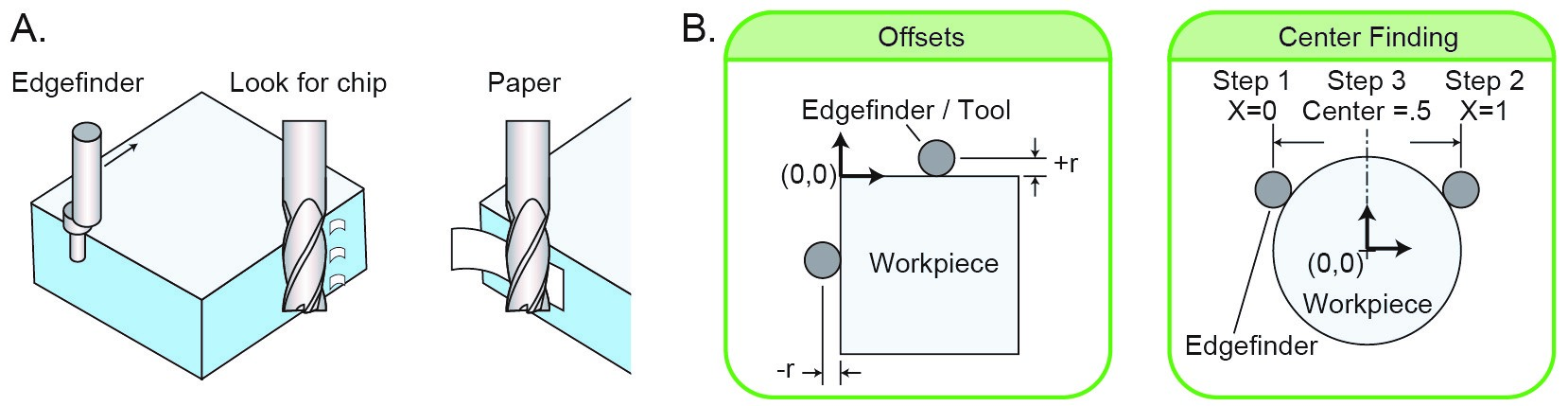
Fig. 1. Four techniques for aligning the tool to the workpiece in the z-axis (from left to right): (i) reflection, (ii) chip, (iii) paper, and (iv) collet technique.
(i) Reflection Technique
Tooling Note: This technique requires a reflective surface (e.g., transparent materials such as PS or PMMA), but otherwise does not require any specific tooling.
Step 1: Start with the tip of the tool slightly above the workpiece, with the spindle turned off. Step 2: Looking from a near planar location with respect to the workpiece, lower the tool until the tool itself comes in contact with its reflection. Step 3: Set this location as z = 0.
Tip: Placing a piece of paper behind the tool will improve contrast, making it easier to identify when the tool contacts the reflection. A magnifying glass can be used to improve visibility.
(ii) Chip Technique
Tooling Note: This technique does not require any specific tooling.
Step 1: Start with the tool slightly above the surface with the spindle running (i.e., the tool should be rotating). Step 2: Lower the tool towards the surface until either (a) a chip is observed, (b) a mark is made on the surface, or (c) a sound is made from the tool cutting the material. Step 3: Set this location as z = 0.
Tip: This method works best for large and flat endmills, and can be more difficult with small endmills or any tool that is pointed or round at the tip. Note that this is a physical contact method, and will blemish the surface.
(iii) Paper Technique
Tooling Note: This technique requires a small piece of paper of known thickness.
Step 1: Start with the tool above the surface with the spindle turned off. Step 2: Place a piece of paper (with known thickness) between the tool and the workpiece. Step 3: While moving the piece of paper back and forth, lower the tool in stepwise increments. Step 4: Continue lowering the tool until it causes resistance to the sliding piece of paper. Step 5: Set this location as z = the thickness of the paper (e.g., .003”)
Tip: Practice more to become comfortable with identifying when the endmill comes in contact with the surface.
(iv) Collet Technique
Tooling Note: This technique requires an ER20 tool holder (#31829, Tormach) from the Tormach Tooling System (TTS) and an ER20 1/8” collet (#30112, Tormach).
Step 1: Place tool in collet and secure using the setscrew on the side. Step 2: Without the spindle running, lower the tool until it is just above the surface. Step 3: Loosen the setscrew and allow the tool to fall into contact with the workpiece. Step 4: Tighten the setscrew. Step 5: Set this location as z = 0.
X-Y Plane Direction
Fig 2. Techniques for aligning the tool in the x–y plane. (A) Illustrations of the (i) edgefinder, (ii) chip, and (iii) paper techniques. (B) Guide to offsetting a tool (left) and finding the center of an object (right).
(i) Edgefinder Technique
Tooling Note: This technique requires an edgefinder (e.g., #02035186, MSC Industrial Supply).
Step 1: Place edgefinder in collet and start spindle (1000 rpm works well with the edgefinder). Step 2: Deflect the tip of the edgefinder so that it lies eccentric to its initial axis. Step 3: Starting with the x-axis, move the edgefinder toward a perpendicular surface. The tip of the edgefinder will become concentric upon contact with surface, and then return to an eccentric position immediately afterward. This sudden “jump” in eccentricity marks the edge. Step 4: Set the current location to either plus or minus the radius of the tip. See Fig. 2B for more details on deciding a positive or negative bias.
Chip Technique
Tooling Note: This technique does not require any specific tooling.
Step 1: Start with the tool near the face of interest with the spindle running (i.e., the tool should be rotating). Step 2: Step the tool towards the surface, until (a) a chip is observed, (b) a mark is made on the surface, or (c) a sound is made from the tool cutting the material. Step 3: Set this location as (plus or minus) the radius of the endmill.
Tip: This method works best for large diameter endmills. Note that this is a physical contact method, and will blemish the surface.
Paper Technique
Tooling Note: This technique requires a small piece of paper of known thickness.
Step1: Start with the tool near the face of interest with the spindle running Step 2: Gripping gently with thumb and fore-finger, or by pressing it against the surface place a piece of paper between the tool and the surface. Step 3: Step the tool towards the surface until the tool pulls the paper. Step 4: Set this location as (plus or minus) the sum of the endmill radius and paper thickness.
Tip: This method works best for large endmills. Caution: Be sure to keep fingers clear of the cutting tool.
Micromilling is a highly efficient method for fabricating microfluidic devices directly in polymeric materials like thermoplastics. A recent review article highlights the use and relevance of micromilling in the field of microfluidics.1 While milling is most popular among machinists, the technique is becoming cheaper and more accessible to many others. Thus, there is a need for disseminating technical know-how for achieving quality micromilled parts. One common technical issue is ensuring flat work surfaces, and eliminating warping and bending of thin plastics during micromilling, which can lead to uneven milling and large errors in feature dimensions. Here we present a simple technique to achieve flat work surfaces – leveled to within 40 μin / in (.04 μm / mm)) – and properly secure thin plastic workpieces to minimize warping. Please refer to the review article by Guckenberger and co-workers for a primer on micromilling
What do I need?
Tools:
CNC mill (PCNC 770, Tormach)
3/8” set screw holder (#31820, Tormach)
Granite block (6” x 12” x 2” Grade AA, Standridge)
Fig. 1 Tooling and Materials. (A) Hardware necessary for setting up the granite block. Assembly of the T-slot clamps is shown in Fig. 2. (B)(Top) Components needed for the drop test indicator: (i) collet/tool holder, (ii) aluminum adapter, (iii) drop test indicator, (iv) screw to attach indicator to the adapter. (Bottom) Side view of the assembled components. (C) Materials needed for adhering workpiece to the block: (i) surface protection tape, (ii) silicone rubber, (iii) transfer tape, (iv) polystyrene sheet.
What do I do?
Preparation: The dial indicator must be affixed to the head of the mill. To do so, mounting brackets can be purchased or custom-made, as we have done using a block of aluminum. This aluminum serves as a simple adapter between the dial indicator and the collet.
Step 1: Place granite block on the milling table. Note that a stiff yet compliant material is necessary between the block and the milling table to allow for minor adjustments. The particle-board feet affixed to the granite block by the manufacturer (Standridge) are sufficient.
Step 2: Assemble the clamps (Fig. 2A), and position the clamps in either a 3-clamp (Fig. 2B) or 4-clamp (Fig. 2C) configuration. The front of the clamp (i.e., the portion that contacts the granite block) should be the same height as or lower than the rear of the clamp.
Step 3: Hand-tighten each clamp, then tighten an addition 1/8th turn using a wrench.
Step 4: Level the granite block by using the drop test indicator to measure the height across the entire block. The following steps are recommended:
a) Lower the indicator onto the center of the block.
b) Move the indicator along x-axis to the two ends of the block, and note the height of both ends.
c) Position the indicator on the high side of the block and tighten the clamps until the height matches the low side.
d) Repeat steps (b) and (c) for the y-axis.
e) Repeat steps (b) to (d) until the block is level to desired tolerance.
f) Tip: When using the 4-clamp configuration, clamps should be equally tightened in pairs to maintain levelness in the other direction.
Fig. 2 (A) T-slot clamp setup configuration. (B) Granite block configuration using three clamps. (C) Granite block configuration using four clamps.
Step 5: (Optional) Apply a protective adhesive film to the workpiece. This will simplify removal of the transfer tape from the workpiece (see Video).
a) Peel a piece of protective adhesive film from the roll of film.
b) Place a piece of silicone rubber on the roll of tape or other cylindrical roll.
c) Place the protective adhesive film on top of the silicone rubber with the adhesive side face up, assuring the tape is flat.
d) Roll the workpiece onto the piece of tape. The silicone rubber will provide compliance below the tape to prevent bubbles in the tape.
e) Press the tape down to make sure it is fully adhered to the workpiece.
Step 6: Apply 2-sided tape or transfer tape to the workpiece
Step 7: Stick the workpiece onto the granite block.
Step 8: (Optional)Use the drop test indicator again to ensure the workpiece is flat.


")


 Demonstration of solder strength b) small electrode stripping as observed when the solder is removed by a strong tug")


