Martin Arundell, Adai Colom Diego, Óscar Castillo, and Josep Samitier
Nanobioengineering group, Institute for Bioengineering of Catalonia (IBEC), Baldiri Reixac 10-12, 08028 Barcelona, Spain
Why is this useful?
This is a very quick and useful method for researchers who do not have access to high tech micro-fabrication facilities and want to try out an idea or a test in a quick, cheap and simple fashion. In this case it is for those of us who want to test certain techniques such as in-channel electrochemical, conductivity or impedance measurements. It also saves time and costs from using high tech fabrication techniques and will aid the researcher in future designs that can then be fabricated the more conventional way in a clean room. In addition, it is a cheap and effective way of introducing undergraduate and masters students to various chip techniques.
What do I need?
- An oven that will go up to about 150 °C
- Metal clamp with smooth surfaces (the clamp surfaces should be at least 25 by 50 mm). Obviously this depends on the size of the chip you require.
- Tungsten 125 µm wire (Advent) and a pair of good pliers
- Platinum 50 µm wire (Advent)
- PMMA 500 µm thick sheets (Goodfellow)
- Solder
- Araldite 2014 epoxy adhesive Glue
- Stanley (utility) knife
What do I do?
1. The first thing to do is to cut the PMMA sheets depending on the sizes you require and your clamp size.
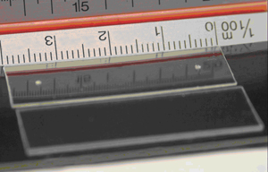
2. Two 1 mm holes should then be drilled on either side of the PMMA device depending on the length of the channel required as shown in Figure 1.
3. Approximate where you would like to place your electrodes and make small slits with a Stanley knife on either edge of one of the PMMA pieces. The number of slits you make depends on how many electrodes you require for your device.
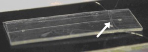
4. The next step is to place the electrodes (as many as you require) onto the chip and carefully position them into the slits, indicated by the arrow in Figure 2. We used 50 µm platinum wires but any size can be used. The larger the wire the easier it is to place the wires on the chip.
5. Then heat up a soldering iron and lightly touch one of the sides of the PMMA chip where the wires are placed in the slits. The soldering iron heats up the wire and slightly melts the PMMA, making it more snug in the slit. This will hold the wire in place and allow you to pull it taught to the other side where it can be permanently bonded in the other PMMA slit. Repeat this step for each electrode.
6. Although the wires are taught it is still possible to re-position them slightly (using the tweezers) depending on the required gap. We were able to get inter-electrode distances down to about 50 µm.
7. The next step is to make a channel and we used a 125 µm tungsten wire (straight cut lengths) for this. See Figure 3.
8. To make the clamping of the device more simple the procedure below should be followed. First, the clamp should be placed on one end so that the PMMA piece with the integrated electrodes can be easily placed on the bottom part of the clamp. The tungsten wire can then be placed on top of the integrated electrode PMMA piece and then a blank PMMA piece placed on top of this. The tungsten wire can then be positioned into place so that it lines up with the drilled holes. The clamp can then be firmly tightened and placed in a pre-heated oven at 140 °C. After 5 minutes the clamp is re-tightened and placed in the oven for a further 10 minutes.
9. The PMMA device can then be removed from the oven and the bonded chip can be removed from the clamp. The tungsten wire can then be removed from the PMMA device and glue can be applied to seal up the open end. When the wire was removed from the PMMA device a channel was formed without disturbing the electrode array. This was carried out a number of times with good reproducibility.
10. Figure 4 shows the resulting channel with integrated electrodes.
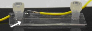
11. Wires can then be attached by using a solder or silver epoxy to the platinum electrode wires. To strengthen the connections it is best to glue the insulation part of the connecting wires to the body of the PMMA, as shown in Figure 5.
What else should I know?
The devices fabricated using the method above were tested using capillary electrophoresis and pressure-driven flow. In both cases they worked very well and the performance of the electrodes was tested using impedance measurements. This worked well by injecting a 1:10 diluted PBS buffer into a concentrated PBS buffer solution and measuring the change in conductivity. No leakages were observed and a good signal resulted from the test. In addition, using the same method, it was also possible to fabricate the chips with cross channels for electrophoretic injection. The cost of materials was approximately €200 for 5 of the 300 x 300 mm x 500 µm thick PMMA sheets from Goodfellow. The 50 µm platinum wire (5 m in length) was ordered from Advent and cost approximately €120 and the 125 µm tungsten straight short wires cost approximately €80 for 100 pieces. Total cost for the wires is about €400 which would make about 100 chips at an approximate cost of €4.00 per chip.


