Colin D. Mansfield, Radoslaw Mazurczyk and Julien Vieillard
Institut des Nanotechnologies de Lyon, Ecole Centrale de Lyon, France
Why is this useful?
Bonding of glass-based lab-on-a-chip (LOC) devices presents a challenging, time-consuming problem, often requiring specialist equipment and skills. Moreover, it is fraught with dangers that if the typically elaborate protocol [1-3] is not strictly followed, then the chip’s channels may leak, ruining an otherwise perfectly good device. Ironically, successful bonding can also be a liability, a chip’s lifetime being reduced due to the difficulties and ambiguity associated with thoroughly cleaning its channels between experiments. Other factors that make bonding of glass-based microdevices problematic include: (i) the inherent nanometre roughness of glass (which renders direct glass-glass bonding a non-trivial task); (ii) low-temperature requirements imposed by possible integration of opto-electronic components; (iii) certain processes, (e.g. ion-exchange waveguide integration) can introduce surface defects (~200 nm in height) that preclude any possibility of glass-to-glass bonding without planarization.
This tip describes a simple, inexpensive and reversible solution to enclose microchannels, using a sheet of polydimethylsiloxane (PDMS). It avoids all the pitfalls mentioned; the natural compliance and adhesion of the PDMS sheet conforms efficiently to the glass substrate’s topography to form a leak-free seal, while the ‘bonding’ is performed at room temperature with very basic equipment. Moreover, since the PDMS layer is easily peeled away from the substrate, there are no consequences if the initial alignment fails and there is full access to the microchannels during cleaning, allowing chips to be recycled.
What do I need?
- Sylgard 184 silicone elastomer kit (DowCorning).
- Flat glass support, preferably with raised edges.
- Measuring cylinder, beaker, plastic stirrer, xylene, paper towels.
- Cutter, ruler, print-off of device geometry, hole punch, tweezers.
- Oven, spin-coater (optional).Mix PDMS and curing agent in a 10:1 weight ratio in a disposable weigh boat.
What do I do?
1. PDMS is messy stuff, so first cover the working area with paper towels to catch any spills.
2. Mix the base polymer and curing agent in a ratio of 10:1 and stir vigorously for 5 minutes to obtain a homogeneous solution. (For a 15 x 15 cm glass support, approximately 16.5 ml and 55 ml total volume produces sheets of thickness 0.75 mm and 2.5 mm respectively).
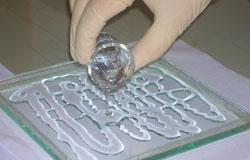
3.Pour this mixture evenly onto the glass support and let it rest for 1 hour to degas and flow (Figure 1). (This process can be accelerated by placing it into a ultrasonic bath for 5 min before pouring).
4. Place the glass support onto a flat surface in the oven and bake for 1 hour at 100 °C. (Alternatively, 24 hours at room temperature or 30 min at 120°C also work well).
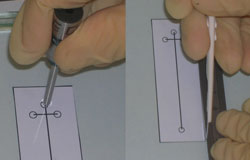
5. Once cooled, place the glass support over your template and scribe around the LOC’s perimeter. If access ports are required, use the punch (e.g. 2 mm outer diameter) to cut out holes, taking care not to leave any shreds (Figure 2).
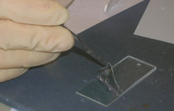
6. Remove the PDMS cover with plastic tweezers and place it over your prepared LOC (Figure 3), ensuring that the side in contact with the support’s surface is face-down. Any trapped air is easily expelled by applying light pressure to the PDMS and pushing it towards the edge. If you are unhappy with the final alignment or cannot remove some trapped air, simply peel off the PDMS layer and repeat this step.
7. For clean-up of PDMS pre-polymer liquid, we have found the solvent xylene works well.
What else should I know?
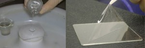
Since it is simple to control the thickness of the PDMS sheet it is also possible to fabricate ‘windows’ of < 50 µm thickness, thereby enclosing the channel and also allowing a delivery/collection fibre to be positioned in very close proximity to the microchannel [4]. The protocol is as described above, however, there is no need for degassing and the layer is prepared using a spin-coating method (1500 rpm, 40 s) onto a glass slide (6 x 6 cm) (Figure 4).
Based upon a PDMS cover of 75 x 25 x 0.75 mm, we estimate the cost of this method to be less than 15 pence/device. This may be especially beneficial to teaching establishments that can use a small number of glass etched devices many times over for practical courses. Although this approach has proven viable in electrophoretic studies,[4] it does have some limitations. Namely, (i) plug flow will be distorted at the glass/PDMS interface, deteriorating separation performance and (ii) proteins are prone to adsorption by the PDMS, worsening the resolution of electrophoresis and hindering the detection of trace proteins. The good news is however, that if data acquired using such a hybrid device shows any signs of promise, your efforts in fabricating a fully glass-bonded chip are certain to be rewarded.
Acknowledgements
Colin Mansfield acknowledges the financial support of the European Community under a Marie Curie Intra-European Fellowship, administered by Dr S Krawczyk.
References
[1] A. Iles, A. Oki and N. Pamme, Bonding of soda-lime glass microchips at low temperature. Microfluid. Nanofluid., 2007, 3, 119-122.
[2] L. Chen, G. Luo, K. Liu, J. Ma, B. Yao, Y. Yan and Y. Wang, Bonding of glass-based microfluidic chips at low- or room-temperature in routine laboratory, Sens. Actuators, B, 2006, 119, 335-344.
[3] N. Chiem, L. Lockyear-Shultz, P. Andersson, C. Skinner and D. Jed Harrison, Room temperature bonding of micromachined glass devices for capillary electrophoresis. Sens. Actuators, B, 2000, 63, 147-152.
[4] R. Mazurczyk, J. Vieillard, A. Bouchard, B. Hannes, S. Krawczyk, A novel concept of the integrated fluorescence detection system and its application in a lab-on-a-chip microdevice. Sens. Actuators B, 2006, 118, 11-19.


