Posted on behalf of Josh Campbell, web writer for CrystEngComm
Quantum dots combine nanocrystals and semiconductors to create materials small enough to show quantum mechanical properties. The excitons (a bound state of an electron and an electron hole) are squeezed together, and if this confinement is in three dimensions, a quantum dot is formed; for two dimensions, a quantum wire, and in one dimension, a quantum well. This squeezing together results in the bandgap of the material becoming highly size dependent, thus tunable and usually blue-shifted. Chalcogenide materials have always drawn research in semiconducting materials, with ternary and quarternary alloys offering even more control over the bandgap while also improving stability or size selectivity.
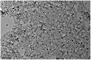
This new paper shows the synthesis of AgBiS2 monodispersed quantum dots that show an extremely high dielectric constant. They were synthesized via the hot injection method, with an average diameter of 8.5nm ± 1.2nm, and the optical band gap energy measured confirmed that strong quantum confinement was taking place. Due to the small size of the nanoparticles, grain boundary effects were expected to dominate the electronic properties. The dielectric constant of the pellets is on the order of 105 and the authors confirmed grain boundaries with large resistances and capacitances gave rise to the huge dielectric constant which has significant implications in the design of similar materials.
Read the paper to find out more:
The synthesis of monodispersed AgBiS2 quantum dots with a giant dielectric constant
Chao Chen, Xiaodong Qiu, Shulin Ji, Chong Jia and Changhui Ye
CrystEngComm, 2013, Advance Article
DOI: 10.1039/C3CE41304G, Communication
 Josh Campbell is a PhD student currently at the University of Southampton studying crystal structure prediction of organic semiconductors. He received his BSc from the University of Bradford.


