ZnO nanostructures have generated much interest recently due to their unique properties, which make them ideal candidates for photo applications such as solar cells, light emitting diodes and field emission displays. While it has been known that Ga doped ZnO shows good field emission properties, there are very few studies on how Ga doping affects the ZnO crystals.
In this paper, the authors investigated Ga doped ZnO nanostructures grown by metal–organic chemical vapor deposition. By varying the growth temperature, Ga concentration and growth time, the authors were able to vary the morphology of the GaZnO nanostructures from wires to a pagoda shape. The formation of the pagodas were also explained via a computational simulation of the growth process.
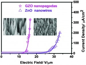
A study of the field emission properties of the GaZnO nanopagodas demonstrated that the geometry of the nanostructure and the density of the pagodas affects the turn-on voltage of the emitters as well as the field enhancement factor. In general, the nanopagodas demonstrated better field emission properties than pure ZnO nanowires.
This study can guide crystal engineers towards designing and producing better GaZnO nanostructures for practical applications.
Find out more from the article:
Experimental and computational insights in the growth of gallium-doped zinc oxide nanostructures with superior field emission properties
Hsien-Ming Chiu, Hsin-Jung Tsai, Wen-Kuang Hsu and Jenn-Ming Wu
CrystEngComm, 2013, Advance Article
DOI: 10.1039/C3CE40101D, Paper


