Mustafa Al-Adhami; Abhay Andar; Elizabeth Tan; Govind Rao; Yordan Kostov*
Center for Advanced Sensor Technology, University of Maryland, Baltimore County, 1000 Hilltop Circle, TRC 252, Baltimore, Maryland, 21250.
*Email: kostov@umbc.edu
Why is this useful?
The demand for microfluidics has steadily increased, due in part to the growing popularity of point-of-care devices [1]. Often, microfluidic chips are fabricated in thermoplastics [1]. Thermoplastics are synthetic polymers that have gained popularity due to their ability to be molded into complex structures [3, 4]. They are often used as a safer and cheaper alternative to glass [3, 4]. However, proper sealing of these devices proves challenging, especially in the field of medical testing, where the demand for reliable devices is high. For example, pressure-sensitive adhesives, common sealants, can limit the size of microfluidic channels; some adhesive can exhibit reactive groups that interfere with analytical processes that run on the chip [5]. Hence, a method of sealing that is free from the aforementioned limitations is needed.
Here, a solvent-based method is presented. Polymethylmethacrylate (PMMA), a thermoplastic, exhibits softening at temperatures above its glass transition temperature (Tg) returning to its original state when cooled. This transition introduces several direct bonding options [6]. However, Tg of PMMA is 115 °C. The pressure required for bonding even at this temperature is fairly high. This can lead to imperfections in the channel dimensions, as the bulk of the material softens. The application of a weak solvent decreases Tg only for the surface of the plastic, thus reducing the required temperature and pressure for the process. The decreased pressure reduces the possibility of channel deformation. Furthermore, as the solvent-induced softening is limited only to the surface (the first few microns), the deeper channel structures are not affected. Hence, a direct solvent bonding method allows for an adhesive-free bonding and avoids a temperature-induced deformation. As a bonus, the mechanical properties of the bond are greatly enhanced [7]. It is worth noting that this approach is valid for microfluidic devices with channel depths greater than 100 microns, typically for devices produced by a direct laser etching.
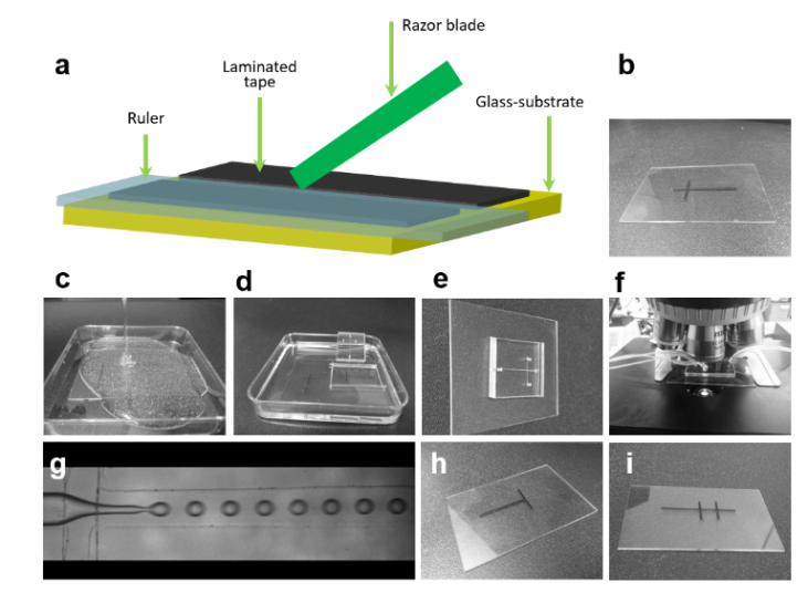
Another advantage of this technique is that it results in the production of sterile devices when the weak solvent is ethanol. They can be manufactured quickly using basic equipment found in any laboratory [7]. To demonstrate this method, PMMA was used along with 90% ethanol as a solvent to bond to other sheet materials such as:
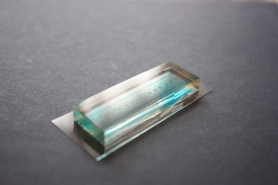
- PMMA sheets,, to manufacture microfluidic mixers and other microfluidic devices for sample processing (Figure 1, a, d) [7];
- ePTFE membranes, to make microfluidic de-bubblers (Figure 1, c); and,
- Cellulose Acetate membranes, to make custom made dialysis devices (Figure 1, b).
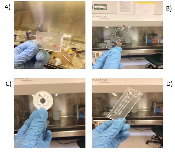
Figure 1. A) Dialysis device B) Redox assay enclosure C) Microfluidic debubbler D) Microfluidic mixer
What do I need?
Materials:
- PMMA sheet, thickness of 1.5 mm (Astra Products)
- PMMA sheet, thickness of 0.2 mm (Astra Products)
- 10K, 20K MWCO Cellulose Acetate membranes (Thermo Fisher Scientific)
- ePTFE membrane (Sterlitech,product number: PTU021350)
- Metal vise (McMaster, product number: 5226A3)
- 1000 grit Sandpaper (McMaster)
- Silicone pad (McMaster)
- KIM-WIPES (Kimberley Clark)
- 2 rectangular metal sheets (McMaster)
- Deionized water
- 90% Ethanol (Decon Labratories, Fisher Scientific, Reagent grade)
Equipment:
- CO2 Laser cutter (Universal laser systems)
- Conventional toaster oven
- Computer aided design (CAD) software (CorelDRAW X4)
What do I do?
- Design devise
- Draw the desired devise design using any available computer aided design (CAD) software.
- Export the CAD file into .dxf file format that is compatible with the laser cutter software.
- Laser cut design
- Place the PMMA sheet of 1.5 mm in thickness onto the bed of the laser cutter.
- Calibrate laser cutter according to sheet thickness.
- Select the correct laser setting in the laser cutter software. It should be height-aligned according to the material and thickness of the sheet.
- Laser cut the core pathway of the design onto the 1.5 mm thickness of PMMA.
- Next, place the other PMMA sheet of 0.2 mm in thickness onto the bed of the laser cutter and repeat points b-c
- Roughen the PMMA sheets
- After laser cutting, there should be a total of three pieces: core channel design (1) and cover sheets (2).
- Rinse the PMMA cutouts with deionized water and wet the sandpaper with tap water.
- Sand the wetted PMMA cutouts in a figure eight-like motion onto the wetted sandpaper until it is milky white. This is to ensure flat conformity on the PMMA sheets to increase bondage.
- Rinse PMMA cutouts with deionized water and dry using “KIM WIPES”.
- Bond the PMMA sheets
- Preheat the temperature-controlled oven to 55 °C. Place the metal vise and the rectangular metal sheets in the oven to preheat as well. Thermal gloves should be used for safety.
- Place a clean sheet of silicone onto a rectangular metal (aluminum) plate.
- Next, place the base cover of the microfluidic cassette on top of the silicone pad in a sandwich manner.
- Spray the 90% ethanol to the base cover sheet until all area is wetted.
- Place the core channel sheet of the PMMA cutout.
- Spray the 90% ethanol to the core channel sheet until the complete area, to be bonded, is wetted.
- Place the final cover sheet of the microfluidic cassette.
- Place the other silicone pad and the other rectangular metal sheet following it.
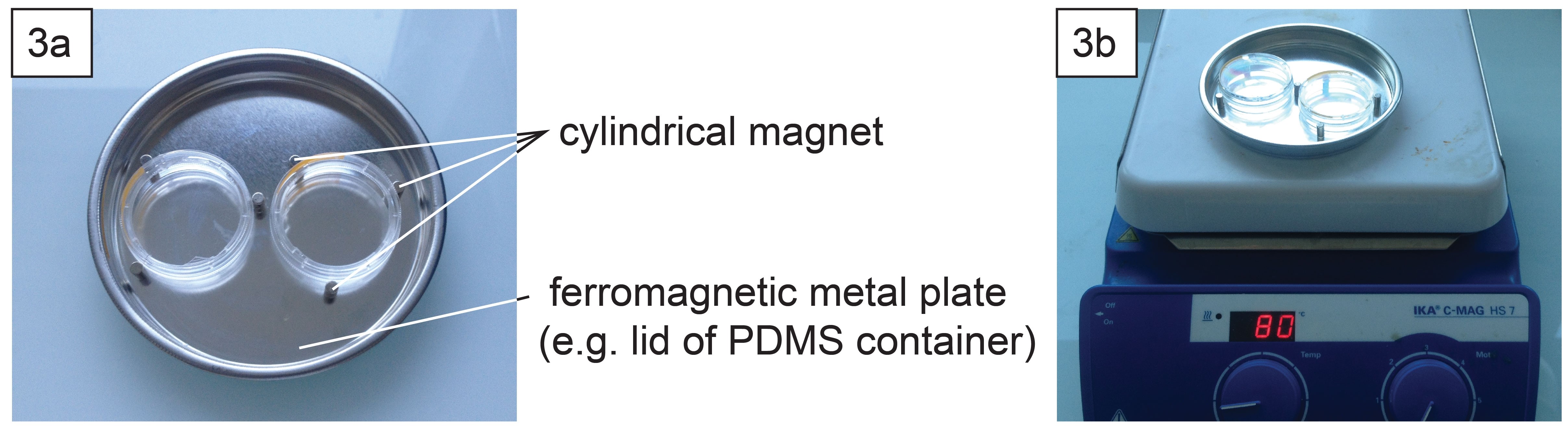
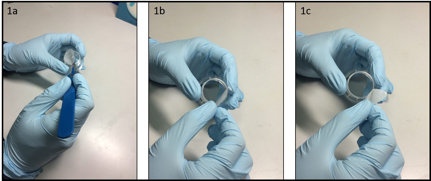
- Place the sandwiched PMMA sheet, silicone pad, and rectangular metal sheet in the metal vise carefully so it does not misalign the cassette (Figure 2.)
- Tighten the vise until can’t turn the lever anymore.
- Place the vise with the microfluidic cassette sandwich into the preheated oven for five minutes. This has to happen before the vise is cooled down.
- Allow to cool to room temperature and remove from metal vise and silicone pad.
- Add inlet and outlet fittings, either glue them on or place them depending on the method of preference
- Bonding PMMA to ePTFE(or cellulose acetate):
- Preheat the temperature-controlled oven to 85°C. Place the metal vise and the rectangular metal sheets in the oven to preheat as well. Thermal gloves should be used for safety.
- Place a clean sheet of silicone onto a rectangular metal (aluminum) plate.
- Next, place the membrane of the microfluidic cassette on top of the silicone pad in a sandwich manner.
- Spray the 90% ethanol on the membrane sheet until all area is wetted.
- Place the core channel sheet of the PMMA cutout.
- Spray the 90% ethanol to the core channel sheet until the complete area, to be bonded, is wetted.
- Place the final PMMA cover sheet of the microfluidic cassette.
- Place the other silicone pad and the other rectangular metal sheet following it.
- Place the sandwiched device, silicone pad, and rectangular metal sheet in the metal vise carefully so it does not misalign the cassette (Figure 2.)
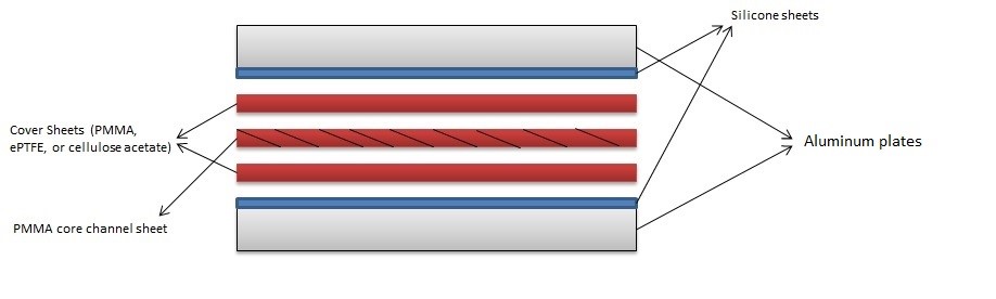
Figure 2. Bonding setup
- Tighten the vise until can’t turn the lever anymore.
- Place the vise with the microfluidic cassette sandwich into the preheated oven for five minutes. This has to happen before the vise is cooled down.
- Allow to cool to room temperature and remove from metal vise and silicone pad and remove the excess membrane if any with scissors.
- Add inlet and outlet fittings, either glue them on or place them depending on the method of preference
What else do I need to know?
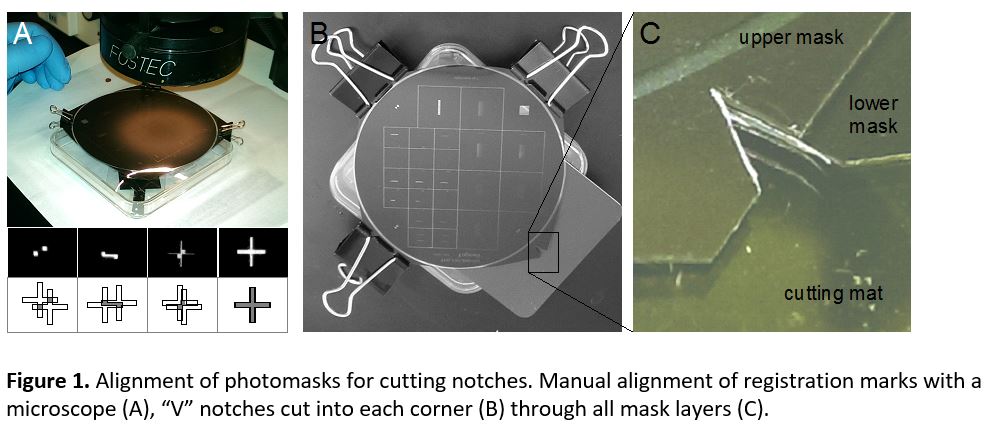
In order to align the sheets on top of each other, three methods were used:
- For PMMA-PMMA devices it is enough to eyeball the alignment. The adhesion forces between the PMMA sheets with ethanol in between are enough to keep them fixed in place.
- An alignment manifold was also fabricated where the machined sheets are placed in. The manifold will prevent the movement of the sheets (Figure 3a.).
- Where the membrane is thick enough to drill a hole through, it is better to use three alignment pins. The pin holes are pre-fabricated when the device is machines. Toothpicks have been used as alignment pins (Figure 3b.).
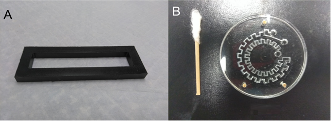
Figure 3. A) Alignment manifold B) 3 wooden pins are used to keep the layers from moving
- For thinner membranes, the machined PMMA is bonded on a slightly bigger membrane. The excess membrane is then removed with scissors.
Acknowledgements
This work was funded by DARPA, Biologically-derived Medicines on Demand (Bio-Mod) Project Grant (N66001-13-C-4023) for financial support.
References
- Sia, S. K., & Kricka, L. J. (2008). Microfluidics and point-of-care testing. Lab on a Chip, 8(12), 1982. doi:10.1039/b817915h
- Materials Used in Microfluidic Devices. (n.d.). SpringerReference. doi: 10.1007 /springerreference_67093
- Liu, K., & Fan, Z. H. (2011). Thermoplastic microfluidic devices and their applications in protein and DNA analysis. The Analyst, 136(7), 1288. doi:10.1039/c0an00969
- Tsao, C., & DeVoe, D. L. (2008). Bonding of thermoplastic polymer microfluidics. Microfluidics and Nanofluidics,6(1), 1-16.doi:10.1007/s10404-008-0361-x
- Hong, T., Ju, W., Wu, M., Tai, C., Tsai, C., & Fu, L. (2010). Rapid prototyping of PMMA microfluidic chips utilizing a CO2 laser. Microfluidics and Nanofluidics, 9(6), 1125-1133. doi:10.1007/s10404-010-0633-0
- Visakh, P. M., & Thomas, S. (2011). Engineering and Specialty Thermoplastics: Nylons: State of Art, New Challenges and Opportunities. Handbook of Engineering and Specialty Thermoplastics, 1-9. doi:10.1002/9781118229064.ch1
- Al-Adhami, M., Tilahun, D., Gurramkonda, C., Rao, G., Kostov, Y (2016) Rapid detection of microbial contamination using a microfluidic devise. In: Biosensors and Biodetection: Methods and Protocols, Second Edition. Ed. A. Rasooly and B. Prickril. Springer.


")