This month sees the following articles in Nanoscale that are in the top ten most accessed in August:
The role of nanomaterials in redox-based supercapacitors for next generation energy storage devices
Xin Zhao, Beatriz Mendoza Sánchez, Peter J. Dobson and Patrick S. Grant
Nanoscale, 2011, 3, 839-855
DOI: 10.1039/c0nr00594k
SnO2 nanosheet hollow spheres with improved lithium storage capabilities
Shujiang Ding and Xiong Wen (David) Lou
Nanoscale, 2011, 3, 3586-3588
DOI: 10.1039/c1nr10581g
Enhanced photocatalytic H2-production activity of graphene-modified titania nanosheets
Quanjun Xiang, Jiaguo Yu and Mietek Jaroniec
Nanoscale, 2011, 3, 3670-3678
DOI: 10.1039/c1nr10610d
Cu2ZnSnS4 nanocrystals and graphene quantum dots for photovoltaics
Jun Wang, Xukai Xin and Zhiqun Lin
Nanoscale, 2011, 3, 3040-3048
DOI: 10.1039/c1nr10425j
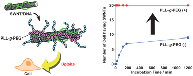
Carbon-based layer-by-layer nanostructures: from films to hollow capsules
Jinkee Hong, Jung Yeon Han, Hyunsik Yoon, Piljae Joo, Taemin Lee, Eunyong Seo, Kookheon Char and Byeong-Su Kim
Nanoscale, 2011, Advance Article
DOI: 10.1039/c1nr10575b
Hierarchical protonated titanate nanostructures for lithium-ion batteries
Yanyan Zhang, Yuxin Tang, Shengyan Yin, Zhiyuan Zeng, Hua Zhang, Chang Ming Li, Zhili Dong, Zhong Chen and Xiaodong Chen
Nanoscale, 2011, Advance Article
DOI: 10.1039/c1nr10522a
Inorganic nanostructures grown on graphene layers
Won Il Park, Chul-Ho Lee, Jung Min Lee, Nam-Jung Kim and Gyu-Chul Yi
Nanoscale, 2011, 3, 3522-3533
DOI: 10.1039/c1nr10370a
Mesoporous silica nanoparticles for bioadsorption, enzyme immobilisation, and delivery carriers
Amirali Popat, Sandy Budi Hartono, Frances Stahr, Jian Liu, Shi Zhang Qiao and Gao Qing (Max) Lu
Nanoscale, 2011, 3, 2801-2818
DOI: 10.1039/c1nr10224a
Nanoengineering and interfacial engineering of photovoltaics by atomic layer deposition
Jonathan R. Bakke, Katie L. Pickrahn, Thomas P. Brennan and Stacey F. Bent
Nanoscale, 2011, 3, 3482-3508
DOI: 10.1039/c1nr10349k
Conjugated polymers/semiconductor nanocrystals hybrid materials—preparation, electrical transport properties and applications
Peter Reiss, Elsa Couderc, Julia De Girolamo and Adam Pron
Nanoscale, 2011, 3, 446-489
DOI: 10.1039/c0nr00403k
Why not take a look at the articles today and blog your thoughts and comments below.
Fancy submitting an article to Nanoscale? Then why not submit to us today or alternatively email us your suggestions.


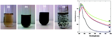
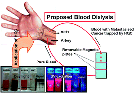 Scientists from India have made blood compatible “hybrid quantum clusters” (HQCs) by combining fluorescent gold clusters with iron-containing superparamagnetic nanoparticles.
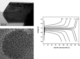 This hierarchical structured LiFePO4/C material could take us a step closer to real and large-scale applications for lithium ion batteries.