Top 25 most-read Nanoscale articles for Q1
Mechanised nanoparticles for drug delivery
Karla K. Cotí, Matthew E. Belowich, Monty Liong, Michael W. Ambrogio, Yuen A. Lau, Hussam A. Khatib, Jeffrey I. Zink, Niveen M. Khashab and J. Fraser Stoddart
DOI: 10.1039/B9NR00162J
Conjugated polymers/semiconductor nanocrystals hybrid materials—preparation, electrical transport properties and applications
Peter Reiss, Elsa Couderc, Julia De Girolamo and Adam Pron
DOI: 10.1039/C0NR00403K
The role of nanomaterials in redox-based supercapacitors for next generation energy storage devices
Xin Zhao, Beatriz Mendoza Sánchez, Peter J. Dobson and Patrick S. Grant
DOI: 10.1039/C0NR00594K
Preparation of functional magnetic nanocomposites and hybrid materials: recent progress and future directions
Silke Behrens
DOI: 10.1039/C0NR00634C
Graphene edges: a review of their fabrication and characterization
Xiaoting Jia, Jessica Campos-Delgado, Mauricio Terrones, Vincent Meunier and Mildred S. Dresselhaus
DOI: 10.1039/C0NR00600A
Current directions in core–shell nanoparticle design
Wolfgang Schärtl
DOI: 10.1039/C0NR00028K
Microwave chemistry for inorganic nanomaterials synthesis
Idalia Bilecka and Markus Niederberger
DOI: 10.1039/B9NR00377K
Solution synthesis of one-dimensional ZnO nanomaterials and their applications
Benjamin Weintraub, Zhengzhi Zhou, Yinhua Li and Yulin Deng
DOI: 10.1039/C0NR00047G
2D materials: to graphene and beyond
Rubén Mas-Ballesté, Cristina Gómez-Navarro, Julio Gómez-Herrero and Félix Zamora
DOI: 10.1039/C0NR00323A
A nanostructured graphene/polyaniline hybrid material for supercapacitors
Hualan Wang, Qingli Hao, Xujie Yang, Lude Lu and Xin Wang
DOI: 10.1039/C0NR00224K
Surface charge of gold nanoparticles mediates mechanism of toxicity
Nicole M. Schaeublin, Laura K. Braydich-Stolle, Amanda M. Schrand, John M. Miller, Jim Hutchison, John J. Schlager and Saber M. Hussain
DOI: 10.1039/C0NR00478B
Controlled assembly of plasmonic colloidal nanoparticle clusters
José M. Romo-Herrera, Ramón A. Alvarez-Puebla and Luis M. Liz-Marzán
DOI: 10.1039/C0NR00804D
Towards multifunctional, targeted drug delivery systems using mesoporous silica nanoparticles – opportunities & challenges
Jessica M. Rosenholm, Cecilia Sahlgren and Mika Lindén
DOI: 10.1039/C0NR00156B
Pitfalls in the characterization of nanoporous and nanosized materials
Claudia Weidenthaler
DOI: 10.1039/C0NR00561D
Sensing with fluorescent nanoparticles
Luca Baù, Paolo Tecilla and Fabrizio Mancin
DOI: 10.1039/C0NR00405G
Upscaling of polymer solar cell fabrication using full roll-to-roll processing
Frederik C. Krebs, Thomas Tromholt and Mikkel Jørgensen
DOI: 10.1039/B9NR00430K
Facile synthesis of metal oxide/reduced graphene oxide hybrids with high lithium storage capacity and stable cyclability
Jixin Zhu, Ting Zhu, Xiaozhu Zhou, Yanyan Zhang, Xiong Wen Lou, Xiaodong Chen, Hua Zhang, Huey Hoon Hng and Qingyu Yan
DOI: 10.1039/C0NR00744G
Surfactant-assisted, shape-controlled synthesis of gold nanocrystals
Junyan Xiao and Limin Qi
DOI: 10.1039/C0NR00814A
Controlled assembly of Fe3O4 magnetic nanoparticles on graphene oxide
Yi Zhang, Biao Chen, Liming Zhang, Jie Huang, Fenghua Chen, Zupei Yang, Jianlin Yao and Zhijun Zhang
DOI: 10.1039/C0NR00776E
Low-toxic and safe nanomaterials by surface-chemical design, carbon nanotubes, fullerenes, metallofullerenes, and graphenes
Liang Yan, Feng Zhao, Shoujian Li, Zhongbo Hu and Yuliang Zhao
DOI: 10.1039/C0NR00647E
TiO2 nanotubes and their application in dye-sensitized solar cells
Poulomi Roy, Doohun Kim, Kiyoung Lee, Erdmann Spiecker and Patrik Schmuki
DOI: 10.1039/B9NR00131J
Small-sized silicon nanoparticles: new nanolights and nanocatalysts
Zhenhui Kang, Yang Liu and Shuit-Tong Lee
DOI: 10.1039/C0NR00559B
Influence of surface plasmon resonance on the emission intermittency of photoluminescence from gold nano-sea-urchins
Yen Hsun Su, Sheng-Lung Tu, Shih-Wen Tseng, Yun-Chorng Chang, Shih-Hui Chang and Wei-Min Zhang
DOI: 10.1039/C0NR00330A
Metallic surfaces with special wettability
Kesong Liu and Lei Jiang
DOI: 10.1039/C0NR00642D
Fabrication of hybrids based on graphene and metal nanoparticles by in situ and self-assembled methods
Fu-An He, Jin-Tu Fan, Fei Song, Li-Ming Zhang and Helen Lai-Wa Chan
DOI: 10.1039/C0NR00672F





 Nanoscale ‘HOT’ paper
 Issue 4
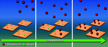 The team recorded the whole dynamic process of the streptavidin–biotin binding reaction. They found that at a streptavidin concentration of 7.6 nM, the binding ratio increased steadily up to nearly 100% within 30 minutes.