Archive for the ‘Nanoscale’ Category

HOT article: On the mechanical and electronic properties of thiolated gold nanocrystals

Whilst undertaking my PhD I was repeatedly warned that the synthesis of nanoparticles was a ‘dark art’ i.e. luck. When, in fact, synthesising these particles actually turned out to be the easy part, whilst the most difficult parts were attempting to achieve stable nanoparticle systems and understanding their resulting properties.

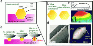
Gold nanocrystals: description and experimental setup.

Even as the field of nanotechnology has undergone considerable expansion there still remain many unanswered fundamental questions. One such question is whether the mechanical and electrical properties of gold nanoparticles are representative of those of the bulk material and how these properties become modified in the presence of an organic coating layer.

Smaali and co-workers have tackled this issue by performing quantitative analysis on the mechanical and electrical properties of thiolated gold nanocrystals. Utilising a recently published procedure, single nanoparticles were grown in a silicon bed with an alkyl-thiol coating on one side and an ohmic contact on the other. To investigate the properties of these nanoparticles, a conducting atomic force microscope (AFM) tip was used, primarily as it offered the ability to interact with the nanocrystals using a variable loaded force with high precision, but also, due to the presence of an ohmic contact, the electrical properties of the nanocrystals and the alkyl-thiol coating could be tested.

Employing AFM measurements and finite elemental analysis (FEA) simulations, the Youngs Modulus of the embedded single nanocrystals was estimated to be 4 times smaller than those of free standing single nanocrystals. The molecular junctions formed between the thiol SAM coating and the individual nanoparticles provided an interesting insight into electronic properties of these materials, with a significant decrease in the tunnel current decay factor and potential barrier height being measured when forces even in the low nN range were applied. These results have been substantiated through FEA and DFT calculations to be a result of strain-induced molecular deformation, which causes a significant impact on the interfacial dipole, resulting in a change in the HOMO position with respect to the Au Fermi energy.

The authors of this study predict that this research could be used as a base model for other studies of functional molecular junctions and mechanical switches, with even small changes in van der Waals forces of a few nN thought to be sufficient to change the electron properties of nanoparticle-based molecular electronic devices.

On the mechanical and electronic properties of thiolated gold nanocrystals
K. Smaali, S. Desbief, G. Foti, T. Frederiksen, D. Sanchez-Portal, A. Arnau, J. P. Nys, P. Leclère, D. Vuillaume and N. Clément
Nanoscale, 2015, 7, 1809-1819. DOI: 10.1039/C4NR06180B

Dr Derek Craig is a guest web writer for the Nanoscale blog. He is a Post Doctoral Research Fellow at the University of St. Andrews based in the fields of Biophotonics and Materials Science. With a background in chemistry, his work mainly focuses on the synthesis of nano to meso materials and the use of imaging techniques to study biological samples.

Digg This
Reddit This
Stumble Now!
Share on Facebook
Bookmark this on Delicious
Share on LinkedIn
Bookmark this on Technorati
Post on Twitter
Google Buzz (aka. Google Reader)

HOT article: Nanovolcanos for Label-Free Sensing Applications

Confined surface plasmon sensors based on strongly coupled disk-in-volcano arrays

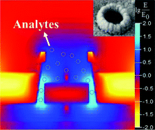
Research concerning plasmonic materials has erupted in recent years due to the unique optical and electrical properties afforded by nanoscale structures. The optical properties of plasmonic materials can be tuned by altering the distance between the gaps of metallic nanostructures, which support surface plasmon resonances (SPR), on a patterned array. The gaps between the nanostructures produce significantly high electric field enhancements that enable the sensitive detection of biomolecules or chemicals within the gaps.

In this HOT article, Ai and co-workers have produced unique plasmonic substrates for sensing applications: disk-in-volcano arrays. The arrays were formed using colloidal lithography techniques wherein polystyrene spheres (PS) were first deposited onto a substrate coated with a photoresist film. Next, active ion etching (RIE) was used to etch the film followed by a vertical silver (Ag) deposition. Finally, the PS and photoresist film were removed with toluene and ethanol, followed by another Ag deposition. The final structures consist of a cavity containing a disk with small nanogaps between the disk and the wall of the “volcano”. The proximity of the disk to the wall results in plasmonic coupling and greatly enhanced electric fields.

The advantages of the confined sensing area of the disk-in-volcano arrays are low background, due to the decreased detection area, and low reagent consumption, making these arrays particularly cost effective. These favorable advantages mean disk-in-volcano arrays show potential in applications such as biosensing, optical and electrical trapping and single-molecule analysis.

Bin Ai, Limin Wang, Helmuth Möhwald, Ye Yua and Gang Zhang
Nanoscale, 2015, Advance Article. DOI: 10.1039/C4NR05206D

Dr Lee Barrett is a guest web writer for the Nanoscale blog. Lee is currently a postdoctoral researcher in the Centre for Molecular Nanometrology at the University of Strathclyde. His research is currently focused on the development of nanoparticle-based sensors and surface enhanced Raman scattering (SERS).

Digg This
Reddit This
Stumble Now!
Share on Facebook
Bookmark this on Delicious
Share on LinkedIn
Bookmark this on Technorati
Post on Twitter
Google Buzz (aka. Google Reader)

HOT article: Tailoring nanoscale properties of tungsten oxide for inkjet printed electrochromic devices

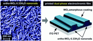
Nanostructured tungsten oxides (WOX) are an important class of materials owing to their electrochromic, photochromic, photochemical and sensing properties. In this study the morphology evolution of WOX nanoparticles was successfully controlled by altering the acidity level and the reaction time of the hydrothermal synthesis. Varying reaction conditions in this manner allowed the nanoparticles to be controlled to suit the desired printability and electrochromic performance.

The “dual-phase” films deposited via inkjet printing technology exhibited values of transmission modulation over the visible and near infrared regions, as compared to the poor electrochromic performance of amorphous films. Films containing synthesized nanoparticles exhibited 2.5 times higher optical modulation and 2 times faster coloration time when compared with pure amorphous films.

As with other areas of nanoscience, the authors stress the importance of tailoring size and morphology of inorganic particles for a desired specification.

Tailoring nanoscale properties of tungsten oxide for inkjet printed electrochromic devices
Pawel Jerzy Wojcik, Lidia Santos, Luis Pereira, Rodrigo Martins and Elvira Fortunato
Nanoscale, 2015, Advance Article. DOI: 10.1039/C4NR05765A

Dr Mike Barrow is a guest web writer for the Nanoscale blog. He currently works as a Postdoctoral Researcher at the University of Liverpool.

Digg This
Reddit This
Stumble Now!
Share on Facebook
Bookmark this on Delicious
Share on LinkedIn
Bookmark this on Technorati
Post on Twitter
Google Buzz (aka. Google Reader)

2014 HOT Nanoscale Papers

We are delighted to showcase a collection of all of the HOT Nanoscale articles published in 2014, as recommended by referees. Congratulations to all of the authors whose articles are featured! Check out a few of them below.

Tracking stem cells in tissue-engineered organs using magnetic nanoparticles
Roxanne Hachani, Mark Lowdell, Martin Birchall and Nguyễn Thi Kim Thanh
Nanoscale, 2013, 5, 11362-11373
DOI: 10.1039/C3NR03861K

Plasmonic Fano resonances in metallic nanorod complexes
Zhong-Jian Yang, Zhong-Hua Hao, Hai-Qing Lin and Qu-Quan Wang
Nanoscale, 2014, 6, 4985-4997
DOI: 10.1039/C3NR06502B

Emerging double helical nanostructures
Meng-Qiang Zhao, Qiang Zhang, Gui-Li Tian and Fei Wei
Nanoscale, 2014, 6, 9339-9354
DOI: 10.1039/C4NR00271G

Graphene–nickel interfaces: a review
Arjun Dahal and Matthias Batzill
Nanoscale, 2014, 6, 2548-2562
DOI: 10.1039/C3NR05279F

Emerging advances in nanomedicine with engineered gold nanostructures
Joseph A. Webb and Rizia Bardhan
Nanoscale, 2014, 6, 2502-2530
DOI: 10.1039/C3NR05112A

Photocatalysts with internal electric fields
Li Li, Paul A. Salvador and Gregory S. Rohrer
Nanoscale, 2014,6, 24-42
DOI: 10.1039/C3NR03998F

Visit the full collection of articles today – why not let us know your thoughts and comments below?

Watch out for posts by our new web writers highlighting HOT articles as they are published.

Digg This
Reddit This
Stumble Now!
Share on Facebook
Bookmark this on Delicious
Share on LinkedIn
Bookmark this on Technorati
Post on Twitter
Google Buzz (aka. Google Reader)

HOT article: Graphene field effect transistor as a probe of electronic structure and charge transfer at organic molecule–graphene interfaces

Graphene has been the focus of intense research over the past couple of decades. Its unique optical, electrical, thermal and mechanical properties mean that graphene is the ideal 2D material for probing interfacial interactions.  The ability to tune the electronic properties of graphene has enabled the highly sensitive detection of various gases, biomolecules and organic molecules. However, the ability to perform selective measurements using such substrates remains a significant barrier needing to be overcome.

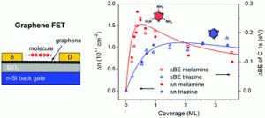
Graphene FET with adsorbed molecules on the surface.

Cervenka and co-workers have devised graphene field electric transistors (FETs) to study the interfacial interactions of two nitrogen hetrocycles, using the knowledge that the electronic structure of graphene can be tuned between n and p-type doping due to the adsorption of electron donating/accepting molecules. Using a combination of electronic transport and XPS measurements this study has shown that molecular recognition can be achieved through the use of FETs due to the presence of non-polar and polar moieties within the analyte molecules.

Significantly, the simplicity of this study opens up the possibility of studying a variety of chemical species selectivity on graphene based sensor devices.

Graphene field effect transistor as a probe of electronic structure and charge transfer at organic molecule–graphene interfaces
Jiri Cervenka, Akin Budi, Nikolai Dontschuk, Alastair Stacey, Anton Tadich, Kevin J. Rietwyk, Alex Schenk, Mark T. Edmonds, Yuefeng Yin, Nikhil Medhekar, Martin Kalbac and Chris I. Pakes
Nanoscale, 2015, 7, 1471-1478. DOI: 10.1039/C4NR05390G

Dr Derek Craig is a guest web writer for the Nanoscale blog. He is a Post Doctoral Research Fellow at the University of St. Andrews based in the fields of Biophotonics and Materials Science. With a background in chemistry, his work mainly focuses on the synthesis of nano to meso materials and the use of imaging techniques to study biological samples.
Digg This
Reddit This
Stumble Now!
Share on Facebook
Bookmark this on Delicious
Share on LinkedIn
Bookmark this on Technorati
Post on Twitter
Google Buzz (aka. Google Reader)

Top 20 Most Accessed Nanoscale Articles in 2014

We are pleased to present a collection of the top 20 most downloaded Nanoscale articles in 2014. Congratulations to all of the authors whose articles are featured!

Atomic resolution imaging of graphene by transmission electron microscopy
Alex W. Robertson and Jamie H. Warner
Nanoscale, 2013, 5, 4079-4093
DOI: 10.1039/C3NR00934C

Nanostructured carbon–metal oxide composite electrodes for supercapacitors: a review
Mingjia Zhi, Chengcheng Xiang, Jiangtian Li, Ming Li and Nianqiang Wu
Nanoscale, 2013, 5, 72-88
DOI: 10.1039/C2NR32040A

Making silica nanoparticle-covered graphene oxide nanohybrids as general building blocks for large-area superhydrophilic coatings
Liang Kou and Chao Gao
Nanoscale, 2011, 3, 519-528
DOI: 10.1039/C0NR00609B

Highly reactive {001} facets of TiO2-based composites: synthesis, formation mechanism and characterization
Wee-Jun Ong, Lling-Lling Tan, Siang-Piao Chai, Siek-Ting Yong and Abdul Rahman Mohamed
Nanoscale, 2014, 6, 1946-2008
DOI: 10.1039/C3NR04655A

Design of advanced porous graphene materials: from graphene nanomesh to 3D architectures
Lili Jiang and Zhuangjun Fan
Nanoscale, 2014, 6, 1922-1945
DOI: 10.1039/C3NR04555B

Photocatalysts with internal electric fields
Li Li, Paul A. Salvador and Gregory S. Rohrer
Nanoscale, 2014, 6, 24-42
DOI: 10.1039/C3NR03998F

Multifunctional superparamagnetic iron oxide nanoparticles: design, synthesis and biomedical photonic applications
Lu Zhang, Wen-Fei Dong and Hong-Bo Sun
Nanoscale, 2013, 5, 7664-7684
DOI: 10.1039/C3NR01616A

Supramolecular self-assemblies as functional nanomaterials
Eric Busseron, Yves Ruff, Emilie Moulin and Nicolas Giuseppone
Nanoscale, 2013, 5, 7098-7140
DOI: 10.1039/C3NR02176A

Focusing on luminescent graphene quantum dots: current status and future perspectives
Lingling Li, Gehui Wu, Guohai Yang, Juan Peng, Jianwei Zhao and Jun-Jie Zhu
Nanoscale, 2013, 5, 4015-4039
DOI: 10.1039/C3NR33849E

Mesoporous silica nanoparticles for bioadsorption, enzyme immobilisation, and delivery carriers
Amirali Popat, Sandy Budi Hartono, Frances Stahr, Jian Liu, Shi Zhang Qiao and Gao Qing (Max) Lu
Nanoscale, 2011, 3, 2801-2818
DOI: 10.1039/C1NR10224A

TEMPO-oxidized cellulose nanofibers
Akira Isogai, Tsuguyuki Saito and Hayaka Fukuzumi
Nanoscale, 2011, 3, 71-85
DOI: 10.1039/C0NR00583E

Photoelectrochemical water oxidation on photoanodes fabricated with hexagonal nanoflower and nanoblock WO3
Nan Wang, Donge Wang, Mingrun Li, Jingying Shi and Can Li
Nanoscale, 2014, 6, 2061-2066
DOI: 10.1039/C3NR05601E

All-solid-state hybrid solar cells based on a new organometal halide perovskite sensitizer and one-dimensional TiO2 nanowire arrays
Jianhang Qiu, Yongcai Qiu, Keyou Yan, Min Zhong, Cheng Mu, He Yan and Shihe Yang
Nanoscale, 2013, 5, 3245-3248
DOI: 10.1039/C3NR00218G

6.5% efficient perovskite quantum-dot-sensitized solar cell
Jeong-Hyeok Im, Chang-Ryul Lee, Jin-Wook Lee, Sang-Won Park and Nam-Gyu Park
Nanoscale, 2011, 3, 4088-4093
DOI: 10.1039/C1NR10867K

Tailor-made directional emission in nanoimprinted plasmonic-based light-emitting devices
G. Lozano, G. Grzela, M. A. Verschuuren, M. Ramezani and J. Gómez Rivas
Nanoscale, 2014, 6, 9223-9229
DOI: 10.1039/C4NR01391C

Improved light absorption and charge transport for perovskite solar cells with rough interfaces by sequential deposition
Lingling Zheng, Yingzhuang Ma, Saisai Chu, Shufeng Wang, Bo Qu, Lixin Xiao, Zhijian Chen, Qihuang Gong, Zhaoxin Wu and Xun Hou
Nanoscale, 2014, 6, 8171-8176
DOI: 10.1039/C4NR01141D

High efficiency electrospun TiO2 nanofiber based hybrid organic–inorganic perovskite solar cell
Sabba Dharani, Hemant Kumar Mulmudi, Natalia Yantara, Pham Thi Thu Trang, Nam Gyu Park, Michael Graetzel, Subodh Mhaisalkar, Nripan Mathews and Pablo P. Boix
Nanoscale, 2014, 6, 1675-1679
DOI: 10.1039/C3NR04857H

Rational morphology control of β-NaYF4:Yb,Er/Tm upconversion nanophosphors using a ligand, an additive, and lanthanide doping
Hyejin Na, Kyoungja Woo, Kipil Lim and Ho Seong Jang
Nanoscale, 2013, 5, 4242-4251
DOI: 10.1039/C3NR00080J

Facile synthesis of water-dispersible Cu2O nanocrystal–reduced graphene oxide hybrid as a promising cancer therapeutic agent
Chengyi Hou, Haocheng Quan, Yourong Duan, Qinghong Zhang, Hongzhi Wang and Yaogang Li
Nanoscale, 2013, 5, 1227-1232
DOI: 10.1039/C2NR32938G

Facile synthesis of lanthanide nanoparticles with paramagnetic, down- and up-conversion properties
Zhengquan Li and Yong Zhang
Nanoscale, 2010, 2, 1240-1243
DOI: 10.1039/C0NR00073F

Why not check out the articles today and let us know your thoughts and comments below?

Digg This
Reddit This
Stumble Now!
Share on Facebook
Bookmark this on Delicious
Share on LinkedIn
Bookmark this on Technorati
Post on Twitter
Google Buzz (aka. Google Reader)

Designing the nanobiointerface of fluorescent nanodiamonds: highly selective targeting of glioma cancer cells

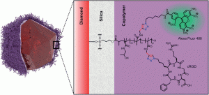
Schematic structure of the fluorescent nanodiamond crystal coated with a biocompatible methacrylamide copolymer grown from an ultrathin silica shell.

Diamonds have always attracted mankind – whether it be in the form of jewellery or knives to cut hard samples! However, a new form of diamond that has attracted scientific fascination in recent times are nanodiamonds, which are tiny nanocrystals of carbon that can be made fluorescent with doping and surface functionalized with various ligands for specific biological targeting. This has immense potential for the bioimaging community, where biologists always seek bright and stable tools for imaging biological processes for longer times without losing signals.

In the present work, Cigler et al. addressed a challenging system, marking integrins (hallmark molecular markers for cancer) present on cancer cells with nanodiamonds. Most nanoparticles aggregate in biological media and on cell surfaces. The authors intelligently coated the diamonds with specific polymers to prevent their aggregation and then functionalized them with multiple cyclic-RGD motifs (a small tripeptide Arg-Gly-Asp that binds strongly to integrins on the cancer cells). The binding was successful and most importantly, specific uptake of these nanodiamonds through integrins was addressed. The best advantage that the nanodiamonds offer is their extremely bright fluorescent properties, which can be explored to image even single nanodiamonds.

Although much fine tuning and multiplexing with different types of diamonds and receptors is still needed, the successful and specific binding and uptake of these nanodiamonds in cancer cells opens new doors, not only for targeted bioimaging, but it could also be applied further to live animals for diagnosis and sensing.

Dr Dhiraj Bhatia

Designing the nanobiointerface of fluorescent nanodiamonds: highly selective targeting of glioma cancer cells
Jitka Slegerova, Miroslav Hajek, Ivan Rehor, Frantisek Sedlak, Jan Stursa, Martin Hruby and Petr Cigler

Nanoscale, 2015, 7, 415-420. DOI: 10.1039/C4NR02776K

Dr Dhiraj Bhatia is a guest web writer for the Nanoscale blog. He is a chemist by training and received his PhD in Chemical Biology of Nucleic Acids from the National Center for Biological Sciences, TIFR India with an outstanding thesis award in 2013. He joined the Chemical Biology department at the Curie Institute, Paris, as an HFSP long term Postdoctoral Fellow and is currently investigating the mechanisms of endocytois using various chemical biology tools.

Digg This
Reddit This
Stumble Now!
Share on Facebook
Bookmark this on Delicious
Share on LinkedIn
Bookmark this on Technorati
Post on Twitter
Google Buzz (aka. Google Reader)

Sunlight-assisted route to antimicrobial plasmonic aminoclay catalysts

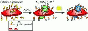
Pathway illustrating the formation of AC@Ag hybrids.

A novel environmentally friendly method has been presented for the synthesis of dual metallic silver (Ag) and gold (Au) nanoparticles on aminoclay nanosheets (ACN). Typically, synthesis of metal nanoparticles requires the aid of toxic reducing agents or complex chemical synthesis and purification.  Baker and co-workers have proposed a one-pot method that utilizes ACN to stabilize precipitating nanoparticles, thus discovering that photochemical reduction using natural unfocused light to be the most time- and energy-efficient method for producing stable nanodispersions in water.

The dual AgAu materials were investigated as catalysts and anti-microbial agents and interestingly showed better activity than analogues synthesised from gold or silver alone. This article highlights the advantages of green synthesis and the potential of hybrid metallic nanoparticles in two different applications. The authors speculate that this generic method could also be expanded to drug delivery, water purification and biological applications.

Sunlight-assisted route to antimicrobial plasmonic aminoclay catalysts
Sudhir Ravula, Jeremy B. Essner, Wendy A. La, Luis Polo-Parada, Roli Kargupta, Garret J. Hull, Shramik Sengupta and Gary A. Baker

Nanoscale, 2015, 7, 86-91. DOI: 10.1039/C4NR04544K

Dr Mike Barrow is a guest web writer for the Nanoscale blog. He currently works as a Postdoctoral Researcher at the University of Liverpool.

Digg This
Reddit This
Stumble Now!
Share on Facebook
Bookmark this on Delicious
Share on LinkedIn
Bookmark this on Technorati
Post on Twitter
Google Buzz (aka. Google Reader)

Poster Prize Winner at the 4th Annual Postgraduate Symposium on Nanotechnology

Congratulations to Richard Archer from the University of Sheffield for winning the Nanoscale and Polymer Chemistry poster prize at the 4th Annual Postgraduate Symposium on Nanotechnology.

Richard won the prize for his poster entitled “Nanospinners: Controlling Rotational Frequency in Self-Phoretic Janus Devices”.

Richard Archer receiving his poster prize from Adam Perriman

The symposium took place at the University of Birmingham on the 15th December 2014 and is aimed at giving early career researchers an opportunity to present their research.

Further information about the symposium can be found on the event website.

Digg This
Reddit This
Stumble Now!
Share on Facebook
Bookmark this on Delicious
Share on LinkedIn
Bookmark this on Technorati
Post on Twitter
Google Buzz (aka. Google Reader)

3D nanoprinting pen

A pen that performs 3D printing on the nanoscale has been developed by scientists in South Korea.

The pen, created by Seongpil Hwang of Korea University and co-workers, amalgamates the precision of atomic force microscopy with a diffusion limited current from a microscopic electrode.

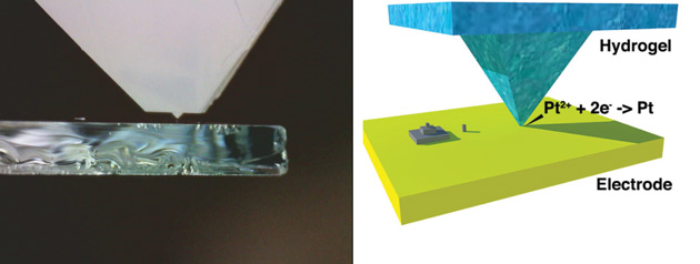
Contact between the pen's tip and a working electrode creates a localised electroactive area for precise electrodeposition

At its tip, the pen has a microscopic hydrogel pyramid, the sharp apex of which is soaked in an electrolyte for electrochemical reactions. A nanometre-scale area for reactant mass transport results from contact between this tip and an ultramicroelectrode. Controlling this contact with a nanopositioning system regulates a faradaic reaction that enables electroplating to give precise nanostructures; in this case 3D structures of platinum were deposited on a gold electrode – some with dimensions less than 100nm.

To read the full article visit the Chemistry World website.

The paper is free to read in Nanoscale until 13 January 2015:

Hydrogel Pen for Electrochemical Reaction and Its Applications for 3D Printing
Hosuk Kang, Seongpil Hwang and Juhyoun Kwak, Nanoscale, 2015, DOI: 10.1039/C4NR06041E

Digg This
Reddit This
Stumble Now!
Share on Facebook
Bookmark this on Delicious
Share on LinkedIn
Bookmark this on Technorati
Post on Twitter
Google Buzz (aka. Google Reader)