Archive for the ‘Nanoscale’ Category

HOT article: Glance into the nanoparticle-imprinted mirror antenna (NIMA)

An ultrahigh-sensitivity plasmonic antenna (NIMA)

Researchers using surface enhanced Raman scattering (SERS) are always on the look out for new substrates that take advantage of coupled metallic nanoparticles to improve sensitivity.  In this HOT article, researchers from Taiwan have introduced NIMAs (nanoparticle (NP)-imprinted mirror antennas) for exactly this purpose.

The researchers deposited Ag on a polycarbonate substrate and used Si molds to create 2D periodic nanostructures, which were then used to create NIMAs by self-assembling Ag nanoparticles onto the Ag mirrors.  The formation of 2D nanoclusters on the mirror results in more intense Raman signals as a result of electromagnetic coupling between the NPs in the clusters. NIMAs have several advantages over other SERS-active substrates. For example, NIMAs gain broadband enhancement from single structures, rather than from various substrates with different morphologies. Also, using a deeper, more consistent structure and tuning the surface plasmon resonance (SPR) modes can drastically improve the SERS enhancement observed from NIMAs.

The researchers have produced a SERS-active substrate that is compatible in the visible to near-infrared regime and is capable of detecting rhodamine 6G at a concentration as low as 10-15 M.  These attractive advantages should be enough for any SERS researcher to reflect on the possibility of adopting NIMAs as a sensing platform in the future.

Chen-Chieh Yu, Yi-Chuan Tseng, Pao-Yun Su, Keng-Te Lin, Chang-Ching Shao, Sin-Yi Chou, Yu-Ting Yen and Hsuen-Li Chen
Nanoscale, 2015, Advance Article. DOI: 10.1039/C4NR05902F.

Dr Lee Barrett is a guest web writer for the Nanoscale blog. Lee is currently a postdoctoral researcher in the Centre for Molecular Nanometrology at the University of Strathclyde. His research is currently focused on the development of nanoparticle-based sensors and surface enhanced Raman scattering (SERS).

Digg This
Reddit This
Stumble Now!
Share on Facebook
Bookmark this on Delicious
Share on LinkedIn
Bookmark this on Technorati
Post on Twitter
Google Buzz (aka. Google Reader)

Poster prize winners at the International Symposium on Bioorganic Chemistry (ISBOC)

Many congratulations to P. S. Pramod and Nilesh Deshpande from the Department of Chemistry at the Indian Institute of Science Education & Research for winning the Nanoscale poster prize at the International Symposium on Bioorganic Chemistry (ISBOC), with their poster entitled “Dextran Nanovesicles for Loading and delivering Anticancer Drugs”.

The conference took place at the Indian Institute of Science Education and Research, Pune, India on the 11-15th  January 2015 and aims to enhance scientific communication between global investigators in chemical biology as well as promote the development of molecular biosciences and related fields. Dr Yamuna Krishnan, one of Nanoscale‘s Associate Editors, was a member of the Organizing Committee. Further information about the conference can be found on the event website.

Digg This
Reddit This
Stumble Now!
Share on Facebook
Bookmark this on Delicious
Share on LinkedIn
Bookmark this on Technorati
Post on Twitter
Google Buzz (aka. Google Reader)

Poster prize winners at the 5th DEA-BRNS Interdisciplinary Symposium on Materials Chemistry (ISMC-2014)

Congratulations to Mr S. J. Pawar from North Maharashtra University and Mr. S. P. Mundinamani from Karnatak University for winning the Nanoscale and Journal of Materials Chemistry A poster prizes, respectively, at the 5th DEA-BRNS Interdisciplinary Symposium on Materials Chemistry (ISMC-2014).

Mr Pawar receiving the Nanoscale poster prize

Mr Pawar won the Nanoscale prize for his poster entitled “Silver Nanoparticle Based Catalytic Conversion of 4-nitrophenol to Paracetamol in Aqueous Medium”, and Mr Mundinamani’s poster entitled “Supercapacitors Based on CdO Thin Films” won the Journal of Materials Chemistry A poster prize.

The conference took place at the Bhabha Atomic Research Centre, Mumbai on the 9-13th December 2014. Further information about the conference can be found on the event website.

ISMC-2014

Digg This
Reddit This
Stumble Now!
Share on Facebook
Bookmark this on Delicious
Share on LinkedIn
Bookmark this on Technorati
Post on Twitter
Google Buzz (aka. Google Reader)

A simple method for the preparation of ultra-small palladium nanoparticles and their utilization for the hydrogenation of terminal alkyne groups to alkanes

(A) Phenyl acetylene penetrating the Pd-NP in the ligand shell and (B) styrene cannot get attached on the ligand capped Pd-NP.

Whether or not we actively think about it, catalysts effect our every day lives.  With applications in automobiles and chemical reactions, catalysts enable modern technologies and have been the subject of much recent research and investment.

When it comes to innovation in catalyst design, Seth et al.’s November 2014 Communication demonstrates a way to create smaller, more selective monolayer-protected palladium nanoparticles (Pd NPs).  While they use a common digestive ripening method, the authors indicate that they perform a unique synthesis step for their Pd NPs; unlike in the traditional synthesis, they do not remove the surfactant during their reflux stage.  Using x-ray diffraction (XRD) and transmission electron microscopy (TEM), nanoparticle sizes were calculated to be 1.5 and ~1.8 nm respectively.  XRD and x-ray photoelectron spectroscopy (XPS) confirmed the presence of Pd(0), while the presence of organic molecules (owing to the ligand shell) was demonstrated via thermogravimetric analysis.

In terms of catalyst action, the authors hypothesize that terminal alkynes can penetrate the ligand shell and undergo hydrogenation to alkenes while other functional groups may not be able to penetrate the shell.  In order to test this hypothesis, they incubated their Pd NPs with phenyl acetylene and styrene and evaluated the results using both Fourier-transform infrared spectroscopy and XPS.  Results indicated that phenyl acetylene interacted with the Pd surface, while the styrene-incubated surfaces showed no such result.  Additionally, according to Seth et al., the MLP Pd NPs could be reused four to five times.

While the authors note that steric hindrance plays a role in this selectivity, they leave the complete mechanism for selectivity for future work.

A simple method for the preparation of ultra-small palladium nanoparticles and their utilization for the hydrogenation of terminal alkyne groups to alkanes
Jhumur Seth, Chandrababu Naidu Kona, Shyamsundar Das and B. L. V. Prasad
Nanoscale, 2015, 7, 872-876. DOI: 10.1039/C4NR04239E

Stephanie E. Vasko is currently a Senior Research Assistant at The Rock Ethics Institute at the Pennsylvania State University in State College. Her research focuses on science communication, STEM education, and the intersections between art, craft, and science.  You can follow her on Twitter at @stephanievasko.

The opinions and views expressed in this piece are those of the author and do not represent or reflect the opinion, views, or policy of the Pennsylvania State University, the Rock Ethics Institute, or the National Science Foundation.
Digg This
Reddit This
Stumble Now!
Share on Facebook
Bookmark this on Delicious
Share on LinkedIn
Bookmark this on Technorati
Post on Twitter
Google Buzz (aka. Google Reader)

HOT article: A facile synthesis of highly luminescent nitrogen-doped graphene quantum dots for the detection of 2,4,6-trinitrophenol in aqueous solution

The last decade observed immense growth in applications of graphene, a carbon allotrope with applications in diverse areas of science, including fluorescent nanoparticles like quantum dots. However, the applications of graphene-based nanodevices in biological contexts have still been a bit slow. This is primarily due to the metal-free nature of graphene nanoparticles, leading to poor fluorescence abilities, and their lack of sensing abilities for various analytes.

Lin et al., in the current work, intelligently overcome these two problems by doping graphene quantum dots with nitrogen-containing species like amines, which not only make the dots much brighter, but also sensitive to various analytes. They show the detection of trinitrophenol, one of the most explosive materials in aqueous solutions, with good sensitivity and a detection limit of 300 nM. The stability of these doped dots to various acidic and alkaline conditions make them suitable for sensing applications in different samples and solutions, especially with biological samples, since the conditions are extremely diverse in these samples. The sensitive detection of trinitrophenol in solutions using simple fluorescence based assays can actually be explored for commercial low cost detectors.

Although much remains to be done to make these dots universally applicable, like doping with different molecules to sense specific analytes, the initial platform technology makes these nanoparticles suitable for applications in biosensing to detect materials like toxins, poisons or even explosives.

Dr Dhiraj Bhatia

A facile synthesis of highly luminescent nitrogen-doped graphene quantum dots for the detection of 2,4,6-trinitrophenol in aqueous solution
Liping Lin, Mingcong Rong, Sisi Lu, Xinhong Song, Yunxin Zhong, Jiawei Yan, Yiru Wang and Xi Chen
Nanoscale, 2015, 7, 1872-1878. DOI: 10.1039/C4NR06365A

Dr Dhiraj Bhatia is a guest web writer for the Nanoscale blog. He is a chemist by training and received his PhD in Chemical Biology of Nucleic Acids from the National Center for Biological Sciences, TIFR India with an outstanding thesis award in 2013. He joined the Chemical Biology department at the Curie Institute, Paris, as an HFSP long term Postdoctoral Fellow and is currently investigating the mechanisms of endocytois using various chemical biology tools.

Digg This
Reddit This
Stumble Now!
Share on Facebook
Bookmark this on Delicious
Share on LinkedIn
Bookmark this on Technorati
Post on Twitter
Google Buzz (aka. Google Reader)

HOT article: On the mechanical and electronic properties of thiolated gold nanocrystals

Whilst undertaking my PhD I was repeatedly warned that the synthesis of nanoparticles was a ‘dark art’ i.e. luck. When, in fact, synthesising these particles actually turned out to be the easy part, whilst the most difficult parts were attempting to achieve stable nanoparticle systems and understanding their resulting properties.

Gold nanocrystals: description and experimental setup.

Even as the field of nanotechnology has undergone considerable expansion there still remain many unanswered fundamental questions. One such question is whether the mechanical and electrical properties of gold nanoparticles are representative of those of the bulk material and how these properties become modified in the presence of an organic coating layer.

Smaali and co-workers have tackled this issue by performing quantitative analysis on the mechanical and electrical properties of thiolated gold nanocrystals. Utilising a recently published procedure, single nanoparticles were grown in a silicon bed with an alkyl-thiol coating on one side and an ohmic contact on the other. To investigate the properties of these nanoparticles, a conducting atomic force microscope (AFM) tip was used, primarily as it offered the ability to interact with the nanocrystals using a variable loaded force with high precision, but also, due to the presence of an ohmic contact, the electrical properties of the nanocrystals and the alkyl-thiol coating could be tested.

Employing AFM measurements and finite elemental analysis (FEA) simulations, the Youngs Modulus of the embedded single nanocrystals was estimated to be 4 times smaller than those of free standing single nanocrystals. The molecular junctions formed between the thiol SAM coating and the individual nanoparticles provided an interesting insight into electronic properties of these materials, with a significant decrease in the tunnel current decay factor and potential barrier height being measured when forces even in the low nN range were applied. These results have been substantiated through FEA and DFT calculations to be a result of strain-induced molecular deformation, which causes a significant impact on the interfacial dipole, resulting in a change in the HOMO position with respect to the Au Fermi energy.

The authors of this study predict that this research could be used as a base model for other studies of functional molecular junctions and mechanical switches, with even small changes in van der Waals forces of a few nN thought to be sufficient to change the electron properties of nanoparticle-based molecular electronic devices.

On the mechanical and electronic properties of thiolated gold nanocrystals
K. Smaali, S. Desbief, G. Foti, T. Frederiksen, D. Sanchez-Portal, A. Arnau, J. P. Nys, P. Leclère, D. Vuillaume and N. Clément
Nanoscale, 2015, 7, 1809-1819. DOI: 10.1039/C4NR06180B

Dr Derek Craig is a guest web writer for the Nanoscale blog. He is a Post Doctoral Research Fellow at the University of St. Andrews based in the fields of Biophotonics and Materials Science. With a background in chemistry, his work mainly focuses on the synthesis of nano to meso materials and the use of imaging techniques to study biological samples.

Digg This
Reddit This
Stumble Now!
Share on Facebook
Bookmark this on Delicious
Share on LinkedIn
Bookmark this on Technorati
Post on Twitter
Google Buzz (aka. Google Reader)

HOT article: Nanovolcanos for Label-Free Sensing Applications

Confined surface plasmon sensors based on strongly coupled disk-in-volcano arrays

Research concerning plasmonic materials has erupted in recent years due to the unique optical and electrical properties afforded by nanoscale structures. The optical properties of plasmonic materials can be tuned by altering the distance between the gaps of metallic nanostructures, which support surface plasmon resonances (SPR), on a patterned array. The gaps between the nanostructures produce significantly high electric field enhancements that enable the sensitive detection of biomolecules or chemicals within the gaps.

In this HOT article, Ai and co-workers have produced unique plasmonic substrates for sensing applications: disk-in-volcano arrays. The arrays were formed using colloidal lithography techniques wherein polystyrene spheres (PS) were first deposited onto a substrate coated with a photoresist film. Next, active ion etching (RIE) was used to etch the film followed by a vertical silver (Ag) deposition. Finally, the PS and photoresist film were removed with toluene and ethanol, followed by another Ag deposition. The final structures consist of a cavity containing a disk with small nanogaps between the disk and the wall of the “volcano”. The proximity of the disk to the wall results in plasmonic coupling and greatly enhanced electric fields.

The advantages of the confined sensing area of the disk-in-volcano arrays are low background, due to the decreased detection area, and low reagent consumption, making these arrays particularly cost effective. These favorable advantages mean disk-in-volcano arrays show potential in applications such as biosensing, optical and electrical trapping and single-molecule analysis.

Bin Ai, Limin Wang, Helmuth Möhwald, Ye Yua and Gang Zhang
Nanoscale, 2015, Advance Article. DOI: 10.1039/C4NR05206D

Dr Lee Barrett is a guest web writer for the Nanoscale blog. Lee is currently a postdoctoral researcher in the Centre for Molecular Nanometrology at the University of Strathclyde. His research is currently focused on the development of nanoparticle-based sensors and surface enhanced Raman scattering (SERS).

Digg This
Reddit This
Stumble Now!
Share on Facebook
Bookmark this on Delicious
Share on LinkedIn
Bookmark this on Technorati
Post on Twitter
Google Buzz (aka. Google Reader)

HOT article: Tailoring nanoscale properties of tungsten oxide for inkjet printed electrochromic devices

Nanostructured tungsten oxides (WOX) are an important class of materials owing to their electrochromic, photochromic, photochemical and sensing properties. In this study the morphology evolution of WOX nanoparticles was successfully controlled by altering the acidity level and the reaction time of the hydrothermal synthesis. Varying reaction conditions in this manner allowed the nanoparticles to be controlled to suit the desired printability and electrochromic performance.

The “dual-phase” films deposited via inkjet printing technology exhibited values of transmission modulation over the visible and near infrared regions, as compared to the poor electrochromic performance of amorphous films. Films containing synthesized nanoparticles exhibited 2.5 times higher optical modulation and 2 times faster coloration time when compared with pure amorphous films.

As with other areas of nanoscience, the authors stress the importance of tailoring size and morphology of inorganic particles for a desired specification.

Tailoring nanoscale properties of tungsten oxide for inkjet printed electrochromic devices
Pawel Jerzy Wojcik, Lidia Santos, Luis Pereira, Rodrigo Martins and Elvira Fortunato
Nanoscale, 2015, Advance Article. DOI: 10.1039/C4NR05765A

Dr Mike Barrow is a guest web writer for the Nanoscale blog. He currently works as a Postdoctoral Researcher at the University of Liverpool.

Digg This
Reddit This
Stumble Now!
Share on Facebook
Bookmark this on Delicious
Share on LinkedIn
Bookmark this on Technorati
Post on Twitter
Google Buzz (aka. Google Reader)

2014 HOT Nanoscale Papers

We are delighted to showcase a collection of all of the HOT Nanoscale articles published in 2014, as recommended by referees. Congratulations to all of the authors whose articles are featured! Check out a few of them below.

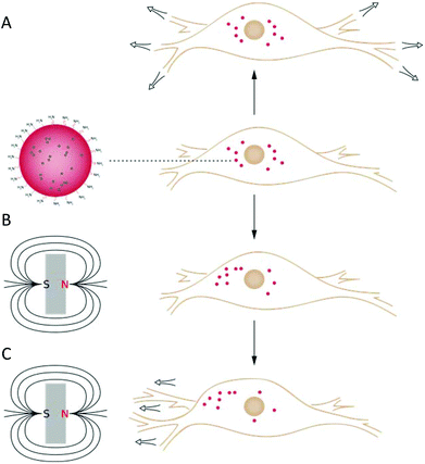
Tracking stem cells in tissue-engineered organs using magnetic nanoparticles
Roxanne Hachani, Mark Lowdell, Martin Birchall and Nguyễn Thi Kim Thanh
Nanoscale, 2013, 5, 11362-11373
DOI: 10.1039/C3NR03861K

Plasmonic Fano resonances in metallic nanorod complexes
Zhong-Jian Yang, Zhong-Hua Hao, Hai-Qing Lin and Qu-Quan Wang
Nanoscale, 2014, 6, 4985-4997
DOI: 10.1039/C3NR06502B

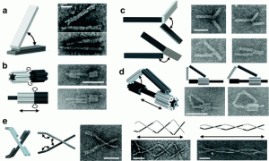
Emerging double helical nanostructures
Meng-Qiang Zhao, Qiang Zhang, Gui-Li Tian and Fei Wei
Nanoscale, 2014, 6, 9339-9354
DOI: 10.1039/C4NR00271G

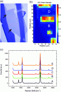
Graphene–nickel interfaces: a review
Arjun Dahal and Matthias Batzill
Nanoscale, 2014, 6, 2548-2562
DOI: 10.1039/C3NR05279F

Emerging advances in nanomedicine with engineered gold nanostructures
Joseph A. Webb and Rizia Bardhan
Nanoscale, 2014, 6, 2502-2530
DOI: 10.1039/C3NR05112A

Photocatalysts with internal electric fields
Li Li, Paul A. Salvador and Gregory S. Rohrer
Nanoscale, 2014,6, 24-42
DOI: 10.1039/C3NR03998F

Visit the full collection of articles today – why not let us know your thoughts and comments below?

Watch out for posts by our new web writers highlighting HOT articles as they are published.

Digg This
Reddit This
Stumble Now!
Share on Facebook
Bookmark this on Delicious
Share on LinkedIn
Bookmark this on Technorati
Post on Twitter
Google Buzz (aka. Google Reader)

HOT article: Graphene field effect transistor as a probe of electronic structure and charge transfer at organic molecule–graphene interfaces

Graphene has been the focus of intense research over the past couple of decades. Its unique optical, electrical, thermal and mechanical properties mean that graphene is the ideal 2D material for probing interfacial interactions.  The ability to tune the electronic properties of graphene has enabled the highly sensitive detection of various gases, biomolecules and organic molecules. However, the ability to perform selective measurements using such substrates remains a significant barrier needing to be overcome.

Graphene FET with adsorbed molecules on the surface.

Cervenka and co-workers have devised graphene field electric transistors (FETs) to study the interfacial interactions of two nitrogen hetrocycles, using the knowledge that the electronic structure of graphene can be tuned between n and p-type doping due to the adsorption of electron donating/accepting molecules. Using a combination of electronic transport and XPS measurements this study has shown that molecular recognition can be achieved through the use of FETs due to the presence of non-polar and polar moieties within the analyte molecules.

Significantly, the simplicity of this study opens up the possibility of studying a variety of chemical species selectivity on graphene based sensor devices.

Graphene field effect transistor as a probe of electronic structure and charge transfer at organic molecule–graphene interfaces
Jiri Cervenka, Akin Budi, Nikolai Dontschuk, Alastair Stacey, Anton Tadich, Kevin J. Rietwyk, Alex Schenk, Mark T. Edmonds, Yuefeng Yin, Nikhil Medhekar, Martin Kalbac and Chris I. Pakes
Nanoscale, 2015, 7, 1471-1478. DOI: 10.1039/C4NR05390G

Dr Derek Craig is a guest web writer for the Nanoscale blog. He is a Post Doctoral Research Fellow at the University of St. Andrews based in the fields of Biophotonics and Materials Science. With a background in chemistry, his work mainly focuses on the synthesis of nano to meso materials and the use of imaging techniques to study biological samples.

Digg This
Reddit This
Stumble Now!
Share on Facebook
Bookmark this on Delicious
Share on LinkedIn
Bookmark this on Technorati
Post on Twitter
Google Buzz (aka. Google Reader)