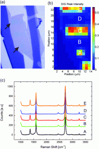
Visual image after EBL treatment, corresponding Raman spectroscopy map of a graphene flake and Raman spectra recorded at different spots on the sample.
Research articles on graphene have been numerously been presented throughout the last decade, indicating the promising future of this material. However, bridging the gap between laboratory research and industrial application remains difficult due to missing specialized large-scale production equipment.
A new article recently published by A. Caglinani et al. introduces an electron beam-based patterning technique using solely widely available clean-room equipment. Based on the findings of the paper, graphene structuring could become a more widespread processing technique.
The researchers developed a patterning process utilizing an industry-standard electron beam lithography system and a standard oven to achieve a resolution of 40 nm.
In the first step, a graphene layer is irradiated by the electron beam which locally generates defects within the crystal lattice. The damage was found by the researchers to be spatially confined to the exposed areas, thus allowing for arbitrary patterns.
The second step comprised etching the irradiated areas by means of hot air at atmospheric pressure. The high defect density (e.g. dangling bonds) induced by the electron beam lead to a large difference in the etch rate compared to the unmodified areas. By exposing the samples for 16 min at 435°C to air, the previously irradiated areas were selectively etched.
In conclusion, the presented process can be used to easily structure graphene layers for future application without the need for specialized equipment. According to the authors, future improvements could reduce the minimum feature size further.
Sebastian Axmann is a guest web-writer for the Nanoscale blog. His interests comprise manufacturing and metrology of nanostructures as well as their usage in current semiconductor devices. He also posts links to interesting research articles on Twitter: @SebastianAxmann.


