Archive for April, 2015

HOT article: The support effect on the size and catalytic activity of thiolated Au25 nanoclusters as precatalysts

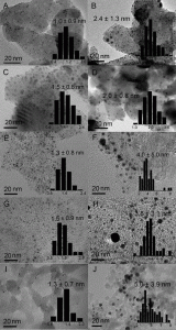
TEM images and size distribution (inset) of various Au25 (1 wt%)/support samples before and after 300 °C calcination.

The use of nanogold (Au NP) catalysts has been widely established for various applications including pharmaceuticals and perfumes.  However, their usage has been limited due to the conventional protocols employed for Au NP synthesis producing polydisperse size ranges, which have proven problematic for identifying catalytic active sites. Recently, this issue has been circumvented through instead using Au nanoclusters (Au NCs), which produce defined cluster sizes with well-defined physiochemical properties. As a direct consequence of being able to exert such control, there have been a number of applications established using such catalysts for processes including CO oxidation, and the oxidation of styrene and cyclohexane. However, whilst the role of the solid support is well established for Au NP catalysis, there currently exists a lack of knowledge on what effect/role the support plays in Au NCs catalysis.

In this study, Fang and co-workers report a systematic assessment of thiolated Au NCs on five different solid supports through examination of the size and electronic structure evolution of the Au NCs during heat treatment, and their catalytic performance when applied to the hydrogenation of nitrobenzene and oxidation of styrene.  The solid supports investigated include hydroxy-apatite (HAP), TiO2 (P25), activated carbon (AC), pyrolyzed grapheme oxide (PGO) and fumed SiO2.

The key findings of these studies establish that AuNCs on HAP and P25 supports presented enhanced activities over the other considered supports. This was found to be due to a number of factors, including reduced NC growth during calcination (heat treatment) following the removal of the thiolated ligands from the nanocluster surface. Further to this, the catalytic activity established during the hydrogenation of nitrobenzene and oxidation of styrene overwhelmingly showed that AuNC-HAP had a greater activity than any of the other supported catalysts. This was found to be due to both the reduced NC growth following heat treatment, and a change in the electronic structure of bound Au, resulting in strengthened metal support interactions.

Although this study has shown HAP to be a superior support in comparison to the others investigated, it should be noted that during heat treatment, an increase in the size of the nanoclusters was still observed.  As a consequence of this, the authors have objectively established improvements which should be made for future studies, including pursuing different support methods and improving the conditions under which the thiolated ligands can be removed from the Au NCs.

The support effect on the size and catalytic activity of thiolated Au25 nanoclusters as precatalysts
Jun Fang, Jingguo Li, Bin Zhang, Xun Yuan, Hiroyuki Asakura, Tsunehiro Tanaka, Kentaro Teramura, Jianping Xie and Ning Yan
Nanoscale, 2015, 7, 6325-6333. DOI: 10.1039/C5NR00549C

Dr Derek Craig is a guest web writer for the Nanoscale blog. He is a Post Doctoral Research Fellow at the University of St. Andrews based in the fields of Biophotonics and Materials Science. With a background in chemistry, his work mainly focuses on the synthesis of nano to meso materials and the use of imaging techniques to study biological samples.


Digg This
Reddit This
Stumble Now!
Share on Facebook
Bookmark this on Delicious
Share on LinkedIn
Bookmark this on Technorati
Post on Twitter
Google Buzz (aka. Google Reader)

Poster prize winner at PhoBiA Annual Nanophotonics International Conference (PANIC 2015)

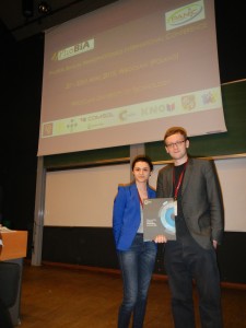
Maciej Bieniek receiving the Nanoscale prize for the best oral presentation at PANIC 2015

Many congratulations to Maciej Bieniek for winning the Nanoscale prize for the best oral presentation at the PhoBiA Annual Nanophotonics International Conference (PANIC 2015).

Maciej, from the Wrocław University of Technology, was chosen by Professors Isabelle Ledoux-Rak, Luana Persano and Robert Luxenhofer to receive the prize for his oral presentation entitled “Two-dimensional topological insulator quantum dots”.

The 6th PhoBiA Annual Nanophotonics International Conference took place from 20th to 23rd April 2015 at Wroclaw University of Technology (Poland). The interdisciplinary conference aims to gather students and young scientists working in the fields of photonics, nanotechnology, biotechnology, materials science and organic electronics in order to enable them to discuss and share their knowledge. The event, organised by students, also featured a number of invited speakers. Further details are available on the conference website.

Nanoscale will be awarding more prizes throughout the year – keep an eye out to find out about the winners!

Digg This
Reddit This
Stumble Now!
Share on Facebook
Bookmark this on Delicious
Share on LinkedIn
Bookmark this on Technorati
Post on Twitter
Google Buzz (aka. Google Reader)

6th International Conference on Nanoscience and Technology (ChinaNANO 2015)

ChinaNANO 2015

Nanoscale is proud to collaborate with the 6th International Conference on Nanoscience and Technology (ChinaNANO 2015), which will be held at the Beijing International Convention Center in Beijing, China on 3-5 September 2015. The conference is organised by the National Center for Nanoscience and Technology, China. Professor Chunli Bai will act as the Chairman of the organising committee.

ChinaNANO 2015 aims to stimulate discussions on the forefront of research in nanoscience and nanotechnology, focusing on the following topics: carbon nanomaterials, inorganic nanomaterials and MOFs, self-assembly and supramolecules, nanocomposites and applications, energy and environmental nanotechnology, nanophotonics and optoelectronics, nanodevices and nanosystems, nanobiotechnology and nanomedicine, nanocharacterization and metrology, modelling and simulation of nanostructures, and the environment, safety and health of nanomaterials.

Submit your abstract now – the deadline is 30 April 2015. For more information, please see the conference website.

Digg This
Reddit This
Stumble Now!
Share on Facebook
Bookmark this on Delicious
Share on LinkedIn
Bookmark this on Technorati
Post on Twitter
Google Buzz (aka. Google Reader)

Disrupting graphene

Scientists across the field of 2D materials have put forward a roadmap to steer graphene research off the drawing board, to a point where it emerges within disruptive technologies that alter people’s lives the world over.

The roadmap is split into 11 science and technology themes including spintronics, biomedical devices and energy conversion and storage. Short-, medium- and long-term targets for technological milestones as well as safety profiles sit alongside the plethora of potential applications.

Interested? Read the full story by Harriet Brewerton in Chemistry World.

The original article is free to access and can be read at:

Andrea C. Ferrari, Francesco Bonaccorso, Vladimir Fal’ko, Konstantin S. Novoselov, Stephan Roche, Peter Bøggild, Stefano Borini, Frank H. L. Koppens, Vincenzo Palermo, Nicola Pugno, José A. Garrido, Roman Sordan, Alberto Bianco, Laura Ballerini, Maurizio Prato, Elefterios Lidorikis, Jani Kivioja, Claudio Marinelli, Tapani Ryhänen, Alberto Morpurgo, Jonathan N. Coleman, Valeria Nicolosi, Luigi Colombo, Albert Fert, Mar Garcia-Hernandez, Adrian Bachtold, Grégory F. Schneider, Francisco Guinea, Cees Dekker, Matteo Barbone, Zhipei Sun, Costas Galiotis, Alexander N. Grigorenko, Gerasimos Konstantatos, Andras Kis, Mikhail Katsnelson, Lieven Vandersypen, Annick Loiseau, Vittorio Morandi, Daniel Neumaier, Emanuele Treossi, Vittorio Pellegrini, Marco Polini, Alessandro Tredicucci, Gareth M. Williams, Byung Hee Hong, Jong-Hyun Ahn, Jong Min Kim, Herbert Zirath, Bart J. van Wees, Herre van der Zant, Luigi Occhipinti, Andrea Di Matteo, Ian A. Kinloch, Thomas Seyller, Etienne Quesnel, Xinliang Feng, Ken Teo, Nalin Rupesinghe, Pertti Hakonen, Simon R. T. Neil, Quentin Tannock, Tomas Löfwander and Jari Kinaret
Nanoscale, 2015, 7, 4598-4810. DOI: 10.1039/C4NR01600A
Digg This
Reddit This
Stumble Now!
Share on Facebook
Bookmark this on Delicious
Share on LinkedIn
Bookmark this on Technorati
Post on Twitter
Google Buzz (aka. Google Reader)

HOT article: Radiolabelled magnetic particles for imaging

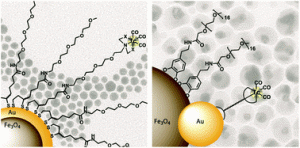
Radiolabelling of core–shell and dumbbell-like nanoparticles

Bi-modal imaging agents are becoming more popular as they can be used to overcome limitations of single imaging modalities. In this work, radiolabelling of gold containing magnetic nanoparticles (Fe3O4-Au) with a nuclear isomer of technetium (99mTc), a commonly used radionuclide for clinical photon emission computed tomography (SPECT), was assessed using two different methods.  In the first approach, Fe3O4-Au core-shell nanoparticles were coated with ligands containing thiol groups to bind to gold and chelator groups for [99mTc(CO)3]+. In the second approach, 99mTc containing ligands were first synthesised, then attached to gold on Fe3O4-Au dumbbell-like nanoparticles. Both synthetic routes were successful in providing a sufficient radiochemical yield on the surface of magnetic nanoparticles, and are ideal candidates as dual magnetic resonance imaging MRI/SPECT imaging agents. In future studies, the authors plan to use the radiolabelled magnetic particles for bimodal imaging of tumours, through attachment of cancer-specific targeting vectors.

99mTc radiolabelling of Fe3O4–Au core–shell and Au–Fe3O4 dumbbell-like nanoparticles
M. Felber and R. Alberto
Nanoscale, 2015, 7, 6653-6660. DOI: 10.1039/C5NR00269A

Dr Mike Barrow is a guest web writer for the Nanoscale blog. He currently works as a Postdoctoral Researcher at the University of Liverpool.

Digg This
Reddit This
Stumble Now!
Share on Facebook
Bookmark this on Delicious
Share on LinkedIn
Bookmark this on Technorati
Post on Twitter
Google Buzz (aka. Google Reader)

HOT article: Scalable and cost effective patterning of graphene layers

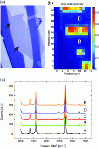
Visual image after EBL treatment, corresponding Raman spectroscopy map of a graphene flake and Raman spectra recorded at different spots on the sample.

Research articles on graphene have been numerously been presented throughout the last decade, indicating the promising future of this material. However, bridging the gap between laboratory research and industrial application remains difficult due to missing specialized large-scale production equipment.

A new article recently published by A. Caglinani et al. introduces an electron beam-based patterning technique using solely widely available clean-room equipment. Based on the findings of the paper, graphene structuring could become a more widespread processing technique.

The researchers developed a patterning process utilizing an industry-standard electron beam lithography system and a standard oven to achieve a resolution of 40 nm.

In the first step, a graphene layer is irradiated by the electron beam which locally generates defects within the crystal lattice. The damage was found by the researchers to be spatially confined to the exposed areas, thus allowing for arbitrary patterns.

The second step comprised etching the irradiated areas by means of hot air at atmospheric pressure. The high defect density (e.g. dangling bonds) induced by the electron beam lead to a large difference in the etch rate compared to the unmodified areas. By exposing the samples for 16 min at 435°C to air, the previously irradiated areas were selectively etched.

In conclusion, the presented process can be used to easily structure graphene layers for future application without the need for specialized equipment. According to the authors, future improvements could reduce the minimum feature size further.

Alberto Cagliani, Niclas Lindvall, Martin Benjamin Barbour Spanget Larsen, David M. A. Mackenzie, Bjarke Sørensen Jessen, Timothy J. Booth and Peter Bøggild
Nanoscale, 2015, 7, 6271-6277. DOI: 10.1039/C4NR07585D

Sebastian Axmann is a guest web-writer for the Nanoscale blog. His interests comprise manufacturing and metrology of nanostructures as well as their usage in current semiconductor devices. He also posts links to interesting research articles on Twitter: @SebastianAxmann.

Digg This
Reddit This
Stumble Now!
Share on Facebook
Bookmark this on Delicious
Share on LinkedIn
Bookmark this on Technorati
Post on Twitter
Google Buzz (aka. Google Reader)