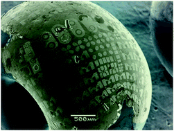
Graphene could find use in next-generation flexible electronic devices thanks to scientists in Taiwan and the US who have developed a low cost and scalable method to pattern graphene onto 3D surfaces.
Flexible electronics are destined to transform the way we manufacture and interact with electronic devices. Graphene’s high electrical conductivity and mechanical stability could prove beneficial in flexible electronic circuits. However, despite its potential, graphene is typically only produced and patterned in research environments with economic barriers hampering its use in commercial applications.
Now, a group led by Mario Hofmann at National Cheng Kung University have demonstrated an easy and scalable approach to depositing high resolution graphene patterns onto surfaces.
Interested to know more? Read the full news article by Michael Parkin in Chemistry World here…
Read the article by Mario Hofmann, Ya-Ping Hsieh, Allen L. Hsu and Jing Kong in Nanoscale:
Scalable, flexible and high resolution patterning of CVD graphene
Mario Hofmann, Ya-Ping Hsieh, Allen L. Hsu and Jing Kong
DOI: 10.1039/C3NR04968J


