Archive for the ‘Fabrication’ Category

A solvent-based method to fabricate PMMA microfluidic devices

Mustafa Al-Adhami; Abhay Andar; Elizabeth Tan; Govind Rao; Yordan Kostov*

Center for Advanced Sensor Technology, University of Maryland, Baltimore County, 1000 Hilltop Circle, TRC 252, Baltimore, Maryland, 21250.

*Email: kostov@umbc.edu

Why is this useful?

The demand for microfluidics has steadily increased, due in part to the growing popularity of point-of-care devices [1].  Often, microfluidic chips are fabricated in thermoplastics [1]. Thermoplastics are synthetic polymers that have gained popularity due to their ability to be molded into complex structures [3, 4]. They are often used as a safer and cheaper alternative to glass [3, 4]. However, proper sealing of these devices proves challenging, especially in the field of medical testing, where the demand for reliable devices is high. For example, pressure-sensitive adhesives, common sealants, can limit the size of microfluidic channels; some adhesive can exhibit reactive groups that interfere with analytical processes that run on the chip [5]. Hence, a method of sealing that is free from the aforementioned limitations is needed.

Here, a solvent-based method is presented. Polymethylmethacrylate (PMMA), a thermoplastic, exhibits softening at temperatures above its glass transition temperature (Tg) returning to its original state when cooled. This transition introduces several direct bonding options [6]. However, Tg of PMMA is 115 °C. The pressure required for bonding even at this temperature is fairly high. This can lead to imperfections in the channel dimensions, as the bulk of the material softens. The application of a weak solvent decreases Tg only for the surface of the plastic, thus reducing the required temperature and pressure for the process. The decreased pressure reduces the possibility of channel deformation. Furthermore, as the solvent-induced softening is limited only to the surface (the first few microns), the deeper channel structures are not affected. Hence, a direct solvent bonding method allows for an adhesive-free bonding and avoids a temperature-induced deformation. As a bonus, the mechanical properties of the bond are greatly enhanced [7]. It is worth noting that this approach is valid for microfluidic devices with channel depths greater than 100 microns, typically for devices produced by a direct laser etching.

Another advantage of this technique is that it results in the production of sterile devices when the weak solvent is ethanol. They can be manufactured quickly using basic equipment found in any laboratory [7]. To demonstrate this method, PMMA was used along with 90% ethanol as a solvent to bond to other sheet materials such as:

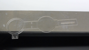
  • PMMA sheets,, to manufacture microfluidic mixers and other microfluidic devices for sample processing (Figure 1, a, d) [7];
  • ePTFE membranes, to make microfluidic de-bubblers (Figure 1, c); and,
  • Cellulose Acetate membranes, to make custom made dialysis devices (Figure 1, b).
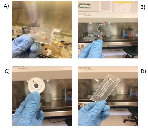
Figure 1. A) Dialysis device B) Redox assay enclosure C) Microfluidic debubbler D) Microfluidic mixer

What do I need?

Materials:

  • PMMA sheet, thickness of 1.5 mm (Astra Products)
  • PMMA sheet, thickness of 0.2 mm (Astra Products)
  • 10K, 20K MWCO Cellulose Acetate membranes (Thermo Fisher Scientific)
  • ePTFE membrane (Sterlitech,product number: PTU021350)
  • Metal vise (McMaster, product number: 5226A3)
  • 1000 grit Sandpaper (McMaster)
  • Silicone pad (McMaster)
  • KIM-WIPES (Kimberley Clark)
  • 2 rectangular metal sheets (McMaster)
  • Deionized water
  • 90% Ethanol (Decon Labratories, Fisher Scientific, Reagent grade)

Equipment:

  • CO2 Laser cutter (Universal laser systems)
  • Conventional toaster oven
  • Computer aided design (CAD) software (CorelDRAW X4)

What do I do?

  1. Design devise
    1. Draw the desired devise design using any available computer aided design (CAD) software.
    2. Export the CAD file into .dxf file format that is compatible with the laser cutter software.
  2. Laser cut design
    1. Place the PMMA sheet of 1.5 mm in thickness onto the bed of the laser cutter.
    2. Calibrate laser cutter according to sheet thickness.
    3. Select the correct laser setting in the laser cutter software. It should be height-aligned according to the material and thickness of the sheet.
    4. Laser cut the core pathway of the design onto the 1.5 mm thickness of PMMA.
    5. Next, place the other PMMA sheet of 0.2 mm in thickness onto the bed of the laser cutter and repeat points b-c
  3. Roughen the PMMA sheets
    1. After laser cutting, there should be a total of three pieces: core channel design (1) and cover sheets (2).
    2. Rinse the PMMA cutouts with deionized water and wet the sandpaper with tap water.
    3. Sand the wetted PMMA cutouts in a figure eight-like motion onto the wetted sandpaper until it is milky white. This is to ensure flat conformity on the PMMA sheets to increase bondage.
    4. Rinse PMMA cutouts with deionized water and dry using “KIM WIPES”.
  4. Bond the PMMA sheets
    1. Preheat the temperature-controlled oven to 55 °C. Place the metal vise and the rectangular metal sheets in the oven to preheat as well. Thermal gloves should be used for safety.
    2. Place a clean sheet of silicone onto a rectangular metal (aluminum) plate.
    3. Next, place the base cover of the microfluidic cassette on top of the silicone pad in a sandwich manner.
    4. Spray the 90% ethanol to the base cover sheet until all area is wetted.
    5. Place the core channel sheet of the PMMA cutout.
    6. Spray the 90% ethanol to the core channel sheet until the complete area, to be bonded, is wetted.
    7. Place the final cover sheet of the microfluidic cassette.
    8. Place the other silicone pad and the other rectangular metal sheet following it.
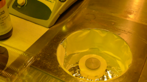
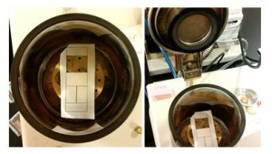
    9. Place the sandwiched PMMA sheet, silicone pad, and rectangular metal sheet in the metal vise carefully so it does not misalign the cassette (Figure 2.)
    10. Tighten the vise until can’t turn the lever anymore.
    11. Place the vise with the microfluidic cassette sandwich into the preheated oven for five minutes. This has to happen before the vise is cooled down.
    12. Allow to cool to room temperature and remove from metal vise and silicone pad.
    13. Add inlet and outlet fittings, either glue them on or place them depending on the method of preference
  5. Bonding PMMA to ePTFE(or cellulose acetate):
    1. Preheat the temperature-controlled oven to 85°C. Place the metal vise and the rectangular metal sheets in the oven to preheat as well. Thermal gloves should be used for safety.
    2. Place a clean sheet of silicone onto a rectangular metal (aluminum) plate.
    3. Next, place the membrane of the microfluidic cassette on top of the silicone pad in a sandwich manner.
    4. Spray the 90% ethanol on the membrane sheet until all area is wetted.
    5. Place the core channel sheet of the PMMA cutout.
    6. Spray the 90% ethanol to the core channel sheet until the complete area, to be bonded, is wetted.
    7. Place the final PMMA cover sheet of the microfluidic cassette.
    8. Place the other silicone pad and the other rectangular metal sheet following it.
    9. Place the sandwiched device, silicone pad, and rectangular metal sheet in the metal vise carefully so it does not misalign the cassette (Figure 2.)

      Figure 2. Bonding setup

    10. Tighten the vise until can’t turn the lever anymore.
    11. Place the vise with the microfluidic cassette sandwich into the preheated oven for five minutes. This has to happen before the vise is cooled down.
    12. Allow to cool to room temperature and remove from metal vise and silicone pad and remove the excess membrane if any with scissors.
    13. Add inlet and outlet fittings, either glue them on or place them depending on the method of preference

What else do I need to know?

In order to align the sheets on top of each other, three methods were used:

  1. For PMMA-PMMA devices it is enough to eyeball the alignment. The adhesion forces between the PMMA sheets with ethanol in between are enough to keep them fixed in place.
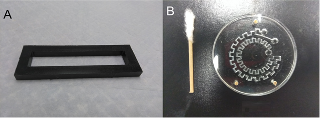
  2. An alignment manifold was also fabricated where the machined sheets are placed in. The manifold will prevent the movement of the sheets (Figure 3a.).
  3. Where the membrane is thick enough to drill a hole through, it is better to use three alignment pins. The pin holes are pre-fabricated when the device is machines. Toothpicks have been used as alignment pins (Figure 3b.).

    Figure 3. A) Alignment manifold B) 3 wooden pins are used to keep the layers from moving

  4. For thinner membranes, the machined PMMA is bonded on a slightly bigger membrane. The excess membrane is then removed with scissors.

Acknowledgements

This work was funded by DARPA, Biologically-derived Medicines on Demand (Bio-Mod) Project Grant (N66001-13-C-4023) for financial support.

References

  • Sia, S. K., & Kricka, L. J. (2008). Microfluidics and point-of-care testing. Lab on a Chip8(12), 1982. doi:10.1039/b817915h
  • Materials Used in Microfluidic Devices. (n.d.). SpringerReference. doi: 10.1007 /springerreference_67093
  • Liu, K., & Fan, Z. H. (2011). Thermoplastic microfluidic devices and their applications in protein and DNA analysis. The Analyst136(7), 1288. doi:10.1039/c0an00969
  • Tsao, C., & DeVoe, D. L. (2008). Bonding of thermoplastic polymer microfluidics. Microfluidics and Nanofluidics,6(1), 1-16.doi:10.1007/s10404-008-0361-x
  • Hong, T., Ju, W., Wu, M., Tai, C., Tsai, C., & Fu, L. (2010). Rapid prototyping of PMMA microfluidic chips utilizing a CO2 laser. Microfluidics and Nanofluidics9(6), 1125-1133. doi:10.1007/s10404-010-0633-0
  • Visakh, P. M., & Thomas, S. (2011). Engineering and Specialty Thermoplastics: Nylons: State of Art, New Challenges and Opportunities. Handbook of Engineering and Specialty Thermoplastics, 1-9. doi:10.1002/9781118229064.ch1
  • Al-Adhami, M., Tilahun, D., Gurramkonda, C., Rao, G., Kostov, Y (2016) Rapid detection of microbial contamination using a microfluidic devise. In: Biosensors and Biodetection: Methods and Protocols, Second Edition. Ed. A. Rasooly and B. Prickril. Springer.
Digg This
Reddit This
Stumble Now!
Share on Facebook
Bookmark this on Delicious
Share on LinkedIn
Bookmark this on Technorati
Post on Twitter
Google Buzz (aka. Google Reader)

A simple, bubble-free cell loading technique for culturing mammalian cells on lab-on-a-chip devices

Sahl Sadeghi1­* and Meltem Elitas1

1 Faculty of Engineering and Natural Sciences, Sabanci University, 34956, Istanbul, Turkey

* Sahl Sadeghi wrote the paper.
 

Purpose

Lab-on-a-chip (LOC) devices significantly contribute different disciplines of science. Polydimethylsiloxane (PDMS) is one of the main materials, which is widely used for the fabrication of biological LOCs, due to its biocompatibility and ease of use. However, PDMS and some other polymeric materials are intrinsically water repellant (or hydrophobic), which results in difficulties in loading and operating LOCs. The eminent consequence of hydrophobicity in LOCs for biological systems is the entrapment of air bubbles in microfluidic channels. Although the oxygen plasma treatment of PDMS reduces the surface hydrophobicity for a certain period of time, the hydrophilic property of PDMS vanishes over time1. The persistent problem of bubbles in the microfluidics led to several studies conducted to overcome it. Some of these solutions suggested implementing bubble traps2,3, surface treatment of LOCs through hydrophilic coatings4, and using actively controlled bubble removal systems 5,6.

Although the aforementioned design complexities are introduced to LOCs in order to reduce the clogging problem caused by the bubbles, these modifications also result in higher production cost, complex operation, and long device preparation time. In many single-cell experiments without losing or damaging the rare cells, these cells needs to be introduce into the LOCs. Here, we present a simple method that enables loading a small number of cells without introducing bubbles in the microfluidics channels.


Materials

·         PDMS (Dow Corning Sylgard 184 Silicon Elastomer Kit)
·         Pipette tips (20-200 ul, Eppendorf, # 3120000917)
·         Pipetman (Gilson, P200, #69989-5)
·         Aqueous ethanol 70% (ZAG Chemistry)
·         Cell culture medium (DMEM, PAN Biotech, #P04-01548)
·         Mammalian cells (MCF7, ATCC-HTB-22)
·         Sterile syringe (BD 10 ml Syringe, Luer-Lok Tip, #300912)
·         Sterile Hamilton syringe (Hamilton, 100 ul SYR, #84884)


Procedure

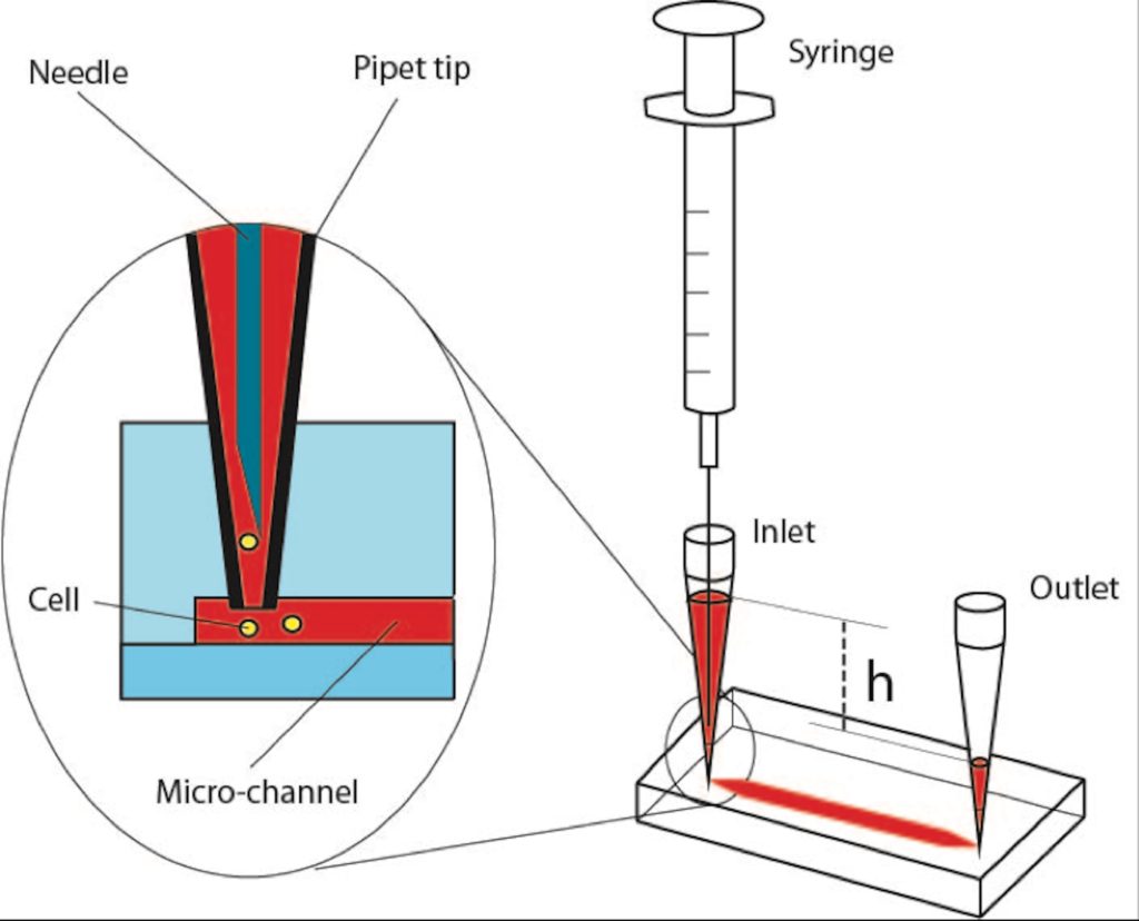
Step 1: Insert two 200-ul pipet tips at the inlet and outlet ports of the PDMS device as illustrated in Figure 1.

Step 2: Introduce a 70% aqueous ethanol into the inlet-pipet tip using a pipetman. Thus, the inner surface of microfluidic channels will be disinfected and the fluid flow will be tested within the micro channels as it is applied in many other protocols for LOCs7,8.

Step 3: Gently apply pressure pressing the pipetman to force ethanol solution flow through the micro channels and cavities of the PDMS device. Take care to avoid applying negative pressure from the outlet-pipet tip, which might create air leakage through the pipet connections. Besides, applying a negative pressure will directly affect the amount of a gas dissolved in the liquid according to Henry’s law9 that might contribute formation of more bubbles inside the micro-channels. The positive pressure will facilitate removal of the air bubbles via dissolving them.

Step 4: After flushing the chip with ethanol solution, inspect the chip to ensure bubble removal. In case of air bubbles, repeat the steps 2 and 3.

Step 5: Fill the syringe (10 ml) with medium or phosphate buffered saline (PBS). Take care to remove the air bubbles inside the syringe, mount and lock the needle on the syringe. Then, flow medium through the needle too make sure the needle is full of medium without any bubble. Insert the needle in the inlet-pipet tip; gently apply positive pressure to replace the ethanol with medium. Next, collect the excess medium from the outlet-pipet tip.

Step 6: Fill the inlet pipet with fresh medium in such a way that due to certain height (h) between the levels of the medium in the inlet and outlet pipet tips, very slow medium flow will be established inside the micro-channels.

Step 7: Load your cells into the Hamilton syringe and take care to ensure that there is no air bubble inside its needle and syringe. Insert the needle of the Hamilton syringe into the inlet-pipet tip as explained in Step 5, Figure 1. Introduce the cells via applying gentle positive pressure to the syringe. Established flow streams in the PDMS chip will deliver the released cells to the desired positions in the chip. Flow rate can be arranged adjusting the applied positive pressure and amount of medium collected in the inlet and outlet pipet tips. The excess supernatant from the outlet-pipet tip can be collected, and fresh medium can be supplied through the inlet-pipet tip during the experiment.


References

  1. Tan, S.H., N.T. Nguyen, Y.C. Chua, and T.G. Kang,. Biomicrofluidics, 2010. 4(3).
  2. Zheng, W.F., Z. Wang, W. Zhang, and X.Y. Jiang,. Lab on a Chip, 2010. 10(21): p. 2906-2910.
  3. Wang, Y., D. Lee, L.S. Zhang, H. Jeon, J.E. Mendoza-Elias, T.A. Harvat, S.Z. Hassan, A. Zhou, D.T. Eddington, and J. Oberholzer, . Biomedical Microdevices, 2012. 14(2): p. 419-426.
  4. Wang, Y.L., C.E. Sims, and N.L. Allbritton,. Lab on a Chip, 2012. 12(17): p. 3036-3039.
  5. Karlsson, J.M., M. Gazin, S. Laakso, T. Haraldsson, S. Malhotra-Kumar, M. Maki, H. Goossens, and W. van der Wijngaart,. Lab on a Chip, 2013. 13(22): p. 4366-4373.
  6. Cortes, D.F., T.-X. Tang, D.G.S. Capelluto, and I.M. Lazar,. Sensors and Actuators B: Chemical, 2017. 243: p. 650-657.
  7. Benavente-Babace, A., D. Gallego-Perez, D.J. Hansford, S. Arana, E. Perez-Lorenzo, and M. Mujika,. Biosensors & Bioelectronics, 2014. 61: p. 298-305.
  8. Yesilkoy, F., R. Ueno, B.X.E. Desbiolles, M. Grisi, Y. Sakai, B.J. Kim, and J. Brugger,. Biomicrofluidics, 2016. 10(1).
  9. Henry, W., Phil. Trans. R. Soc. Lond., 1803. 93: 29–274.

Figure 1 – Schematic of cell loading procedure in a microfluidic PDMS device.


Digg This
Reddit This
Stumble Now!
Share on Facebook
Bookmark this on Delicious
Share on LinkedIn
Bookmark this on Technorati
Post on Twitter
Google Buzz (aka. Google Reader)

Micromilling Techniques II: Tool Alignment

David J. Guckenberger1, Theodorus E. de Groot1, Alwin M.D. Wan2, David J. Beebe1 and Edmond W. K. Young2,*

1 Department of Biomedical Engineering, Wisconsin Institutes for Medical Research, University of Wisconsin-Madison, Madison, WI, USA

2 Department of Mechanical and Industrial Engineering, University of Toronto, 5 King’s College Road, MC313, Toronto, ON, Canada.

* Corresponding Author, E-mail: eyoung@mie.toronto.ca; Tel: +1(416) 978 1521

Why is this useful?


­­­­­­­­­­Micromilling is a highly efficient method for fabricating microfluidic devices directly in polymeric materials like thermoplastics. Please see the review article by Guckenberger and co-workers for a primer on micromilling.1 After securing your workpiece to the milling table,2 the next step in the milling process is to align the tool to the workpiece, thereby defining the coordinate origin. Many high-end mills designed for micromilling have automated tool alignment systems. However, lower cost mills that are also capable of milling microdevices may not have tool alignment systems, and the user must therefore manually align the tool to the workpiece to the desired accuracy. Here we present several alignment techniques that are low cost and can be performed by minimally trained users. We divide tool alignment into two separate directions: the vertical z-axis direction, and the planar x-y plane direction.

What do I need?


  • CNC Mill (PCNC 770, Tormach)
  • Tool, e.g. endmill of choice
  • Workpiece (properly secured to milling table, see ref. [2])

Specific tooling or materials required for each technique are referenced separately below, under the “Tooling Note”.

What do I do?


Z-axis Direction

Fig. 1. Four techniques for aligning the tool to the workpiece in the z-axis (from left to right): (i) reflection, (ii) chip, (iii) paper, and (iv) collet technique.


(i) Reflection Technique

Tooling Note: This technique requires a reflective surface (e.g., transparent materials such as PS or PMMA), but otherwise does not require any specific tooling.


Step 1: Start with the tip of the tool slightly above the workpiece, with the spindle turned off.
Step 2: Looking from a near planar location with respect to the workpiece, lower the tool until the tool itself comes in contact with its reflection.
Step 3: Set this location as z = 0.

Tip:         Placing a piece of paper behind the tool will improve contrast, making it easier to identify when the tool contacts the reflection. A magnifying glass can be used to improve visibility.


(ii) Chip Technique

Tooling Note: This technique does not require any specific tooling.


Step 1: Start with the tool slightly above the surface with the spindle running (i.e., the tool should be rotating).
Step 2: Lower the tool towards the surface until either (a) a chip is observed, (b) a mark is made on the surface, or (c) a sound is made from the tool cutting the material.
Step 3: Set this location as z = 0.

Tip:      This method works best for large and flat endmills, and can be more difficult with small endmills or any tool that is pointed or round at the tip. Note that this is a physical contact method, and will blemish the surface.


(iii) Paper Technique

Tooling Note: This technique requires a small piece of paper of known thickness.


Step 1: Start with the tool above the surface with the spindle turned off.
Step 2: Place a piece of paper (with known thickness) between the tool and the workpiece.
Step 3: While moving the piece of paper back and forth, lower the tool in stepwise increments.
Step 4: Continue lowering the tool until it causes resistance to the sliding piece of paper.
Step 5: Set this location as z = the thickness of the paper (e.g., .003”)

Tip:      Practice more to become comfortable with identifying when the endmill comes in contact with the surface.
(iv) Collet Technique

Tooling Note: This technique requires an ER20 tool holder (#31829, Tormach) from the Tormach Tooling System (TTS) and an ER20 1/8” collet (#30112, Tormach).


Step 1: Place tool in collet and secure using the setscrew on the side.
Step 2: Without the spindle running, lower the tool until it is just above the surface.
Step 3: Loosen the setscrew and allow the tool to fall into contact with the workpiece.
Step 4: Tighten the setscrew.
Step 5: Set this location as z = 0.


X-Y Plane Direction

Fig 2. Techniques for aligning the tool in the xy plane. (A) Illustrations of the (i) edgefinder, (ii) chip, and (iii) paper techniques. (B) Guide to offsetting a tool (left) and finding the center of an object (right).


(i) Edgefinder Technique

Tooling Note:
This technique requires an edgefinder (e.g., #02035186, MSC Industrial Supply).


Step 1: Place edgefinder in collet and start spindle (1000 rpm works well with the edgefinder).
Step 2: Deflect the tip of the edgefinder so that it lies eccentric to its initial axis.
Step 3: Starting with the x-axis, move the edgefinder toward a perpendicular surface. The tip of the edgefinder will become concentric upon contact with surface, and then return to an eccentric position immediately afterward. This sudden “jump” in eccentricity marks the edge.
Step 4: Set the current location to either plus or minus the radius of the tip. See Fig. 2B for more details on deciding a positive or negative bias.

Chip Technique

Tooling Note: This technique does not require any specific tooling.


Step 1: Start with the tool near the face of interest with the spindle running (i.e., the tool should be rotating).
Step 2: Step the tool towards the surface, until (a) a chip is observed, (b) a mark is made on the surface, or (c) a sound is made from the tool cutting the material.
Step 3: Set this location as (plus or minus) the radius of the endmill.

Tip:      This method works best for large diameter endmills. Note that this is a physical contact method, and will blemish the surface.

Paper Technique

Tooling Note: This technique requires a small piece of paper of known thickness.


Step 1: Start with the tool near the face of interest with the spindle running
Step 2: Gripping gently with thumb and fore-finger, or by pressing it against the surface place a piece of paper between the tool and the surface.
Step 3: Step the tool towards the surface until the tool pulls the paper.
Step 4: Set this location as (plus or minus) the sum of the endmill radius and paper thickness.

Tip:                  This method works best for large endmills.
Caution:          Be sure to keep fingers clear of the cutting tool.

References


1.   Guckenberger DJ, de Groot T, Wan AMD, Beebe DJ, Young EWK, “Micromilling: A method for ultra-rapid prototyping of plastic microfluidic devices”, Lab on a Chip, DOI:10.1039/c5lc00234f (2015).

2.   Guckenberger DJ, de Groot T, Wan AMD, Beebe DJ, Young EWK, “Micromilling Techniques I: Securing Thin Plastic Workpieces for Precise Milling”, Chips & Tips (2015).

Digg This
Reddit This
Stumble Now!
Share on Facebook
Bookmark this on Delicious
Share on LinkedIn
Bookmark this on Technorati
Post on Twitter
Google Buzz (aka. Google Reader)

Micromilling Techniques I: Securing Thin Plastic Workpieces for Precise Milling

David J. Guckenberger1, Theodorus E. de Groot1, Alwin M.D. Wan2, David J. Beebe1 and Edmond W. K. Young2,*

1 Department of Biomedical Engineering, Wisconsin Institutes for Medical Research, University of Wisconsin-Madison, Madison, WI, USA

2 Department of Mechanical and Industrial Engineering, University of Toronto, 5 King’s College Road, MC313, Toronto, ON, Canada.

* Corresponding Author, E-mail: eyoung@mie.toronto.ca; Tel: +1(416) 978 1521

Why is this useful?


Micromilling is a highly efficient method for fabricating microfluidic devices directly in polymeric materials like thermoplastics. A recent review article highlights the use and relevance of micromilling in the field of microfluidics.1 While milling is most popular among machinists, the technique is becoming cheaper and more accessible to many others. Thus, there is a need for disseminating technical know-how for achieving quality micromilled parts. One common technical issue is ensuring flat work surfaces, and eliminating warping and bending of thin plastics during micromilling, which can lead to uneven milling and large errors in feature dimensions. Here we present a simple technique to achieve flat work surfacesleveled to within 40 μin / in (.04 μm / mm)) – and properly secure thin plastic workpieces to minimize warping. Please refer to the review article by Guckenberger and co-workers for a primer on micromilling

What do I need?


Tools:

  • CNC mill                                 (PCNC 770, Tormach)
  • 3/8” set screw holder       (#31820, Tormach)
  • Granite block                        (6” x 12” x 2” Grade AA, Standridge)
  • T-slot clamps                        (#32580, Tormach)
  • Drop test indicator             (#24-315-4, SPI)
  • Wrench                                    (choose appropriate size for clamps)

Materials:

  • Plastic workpiece                        (e.g., polystyrene, cyclo-olefin copolymer (COC), PMMA)
  • Surface protection tape            (#6092A24, McMaster-Carr)
  • Two-sided or transfer tape      (#9472LE, 3M)
  • Silicone rubber, 1/16” thick    (#8632K41 – Durometer Hardness: 40A, McMaster-Carr)

Fig. 1 Tooling and Materials. (A) Hardware necessary for setting up the granite block. Assembly of the T-slot clamps is shown in Fig. 2. (B) (Top) Components needed for the drop test indicator: (i) collet/tool holder, (ii) aluminum adapter, (iii) drop test indicator, (iv) screw to attach indicator to the adapter. (Bottom) Side view of the assembled components. (C) Materials needed for adhering workpiece to the block: (i) surface protection tape, (ii) silicone rubber, (iii) transfer tape, (iv) polystyrene sheet.

What do I do?


Preparation: The dial indicator must be affixed to the head of the mill. To do so, mounting brackets can be purchased or custom-made, as we have done using a block of aluminum. This aluminum serves as a simple adapter between the dial indicator and the collet.

Step 1: Place granite block on the milling table. Note that a stiff yet compliant material is necessary between the block and the milling table to allow for minor adjustments. The particle-board feet affixed to the granite block by the manufacturer (Standridge) are sufficient.

Step 2: Assemble the clamps (Fig. 2A), and position the clamps in either a 3-clamp (Fig. 2B) or 4-clamp (Fig. 2C) configuration. The front of the clamp (i.e., the portion that contacts the granite block) should be the same height as or lower than the rear of the clamp.

Step 3: Hand-tighten each clamp, then tighten an addition 1/8th turn using a wrench.

Step 4: Level the granite block by using the drop test indicator to measure the height across the entire block. The following steps are recommended:

a)      Lower the indicator onto the center of the block.
b)      Move the indicator along x-axis to the two ends of the block, and note the height of both ends.
c)      Position the indicator on the high side of the block and tighten the clamps until the height matches the low side.
d)     Repeat steps (b) and (c) for the y-axis.
e)      Repeat steps (b) to (d) until the block is level to desired tolerance.
f)       Tip: When using the 4-clamp configuration, clamps should be equally tightened in pairs to maintain levelness in the other direction.

Fig. 2 (A) T-slot clamp setup configuration. (B) Granite block configuration using three clamps. (C) Granite block configuration using four clamps.

Step 5: (Optional) Apply a protective adhesive film to the workpiece. This will simplify removal of the transfer tape from the workpiece (see Video).

a)      Peel a piece of protective adhesive film from the roll of film.
b)      Place a piece of silicone rubber on the roll of tape or other cylindrical roll.
c)      Place the protective adhesive film on top of the silicone rubber with the adhesive side face up, assuring the tape is flat.
d)     Roll the workpiece onto the piece of tape. The silicone rubber will provide compliance below the tape to prevent bubbles in the tape.
e)      Press the tape down to make sure it is fully adhered to the workpiece.

Step 6: Apply 2-sided tape or transfer tape to the workpiece

Step 7: Stick the workpiece onto the granite block.

Step 8: (Optional) Use the drop test indicator again to ensure the workpiece is flat.

References


1.   Guckenberger DJ, de Groot T, Wan AMD, Beebe DJ, Young EWK, “Micromilling: A method for ultra-rapid prototyping of plastic microfluidic devices”, Lab on a Chip, DOI:10.1039/c5lc00234f (2015).

Digg This
Reddit This
Stumble Now!
Share on Facebook
Bookmark this on Delicious
Share on LinkedIn
Bookmark this on Technorati
Post on Twitter
Google Buzz (aka. Google Reader)

A simple and inexpensive device to remove edge beads

Markus Ludwig and Seth Fraden

Martin A. Fisher School of Physics, Brandeis University, Waltham, Massachusetts 02454, United States

Why is this useful?


To achieve high resolution and high aspect ratio features in contact lithography it is necessary to have the photomask in direct contact with the photoresist during the exposure. This is impeded by the formation of edge beads on the edge of the wafer, which can measure multiples of the nominal resist thickness [1].

Dedicated spin coaters remove edge beads automatically just after spin coating. However, during soft baking, a new edge bead forms due to the coffee ring effect [2]. It is therefore recommended, especially for thicker resist films, to remove the edge bead not before, but after soft baking [3].

Edge bead removal is not critical on single layer devices. However, for multi level designs, edge bead removal can improve the feature resolution significantly. This is especially the case if the first layer of resist is thick and the second layer is thin.

This article presents the fabrication and use of a simple and inexpensive device to reliably remove edge beads by solvent spraying.

What do I need?


Materials:

  • 100 ml round media storage bottle GL45
  • Diba Labware bottle cap Q series GL45 2 x 1/4 -28 ports with valves (00945Q-2V)
  • acrylic sheet, 12” x 6”, 3/16” thick
  • polyethylene sheet, 1/16 “ thick
  • 3x AAA battery pack with on/off switch + batteries
  • Parker micro diaphragm pump T2-05 IC (3/32 ID)
  • 2x ¼-28 to barbed 3/32 ID fitting
  • silicone tubing  0.078” ID, 50 cm length
  • 2x flat head machine screw 4-40 3/8 + nuts
  • 2x socket head machine screw 6-32 3/8 + nuts + washers
  • stainless steel blunt needle with 27 gauge Luer polypropylene hub, 1/2″ length
  • cable tie 4”
  • polypropylene tube fitting, male Luer slip to barbed coupler, 3/32″ tube ID

Tools:

  • hot air gun (Aoyue 968a+)
  • laser cutter (40W/45W CO2 Hobby Laser by Full Spectrum Laser) or scroll saw, drill press and drill bits
  • soldering iron (Aoyue 968a+) and solder

What do I do?


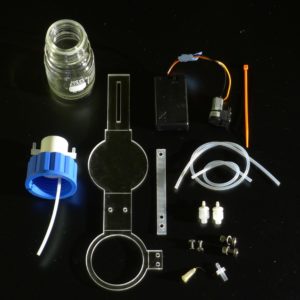
To build the edge bead remover, first prepare all components as shown in figure 1.

Cut the acrylic sheet and the polypropylene sheet and drill the holes as indicated in the schematic1.pdf or schematic1.dwg (AutoCAD) file. Solder battery pack wires to the pump. Then follow the instructions in video 1.

Figure 1: Materials needed

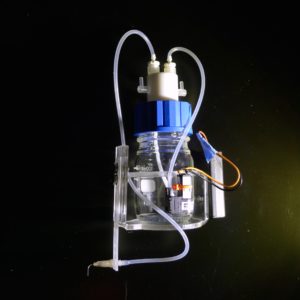
Figure 2: Assembled device

Edge bead removal (follow the instructions in video 2):

  1. Spin coat wafer, soft bake and cool down.
  2. Center the wafer on spin coater and spin at 700 rpm. The optional centering tool used in the video was 3D printed on a formlabs form one 3D printer. (Use centering tool.stl file to reprint)
  3. Turn on pump, open pump valve to pressurize bottle, position nozzle over edge bead.
  4. Open spray valve and dissolve edge bead
  5. Sweep outwards slowly and keep spraying for another 15 seconds.
  6. Turn off spray valve and ramp up to 2000 rpm for 10 sec.
  7. Turn off pump and close both valves. Developer may remain in the bottle and in the tubing.
  8. Wafer does not have to be baked again and can be exposed immediately.

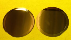
Figure 3: SU8 coated 3” wafer before (left) and after edge bead removal (right).

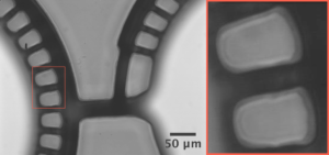
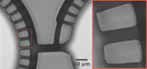
Figure 4: Comparison of feature resolution

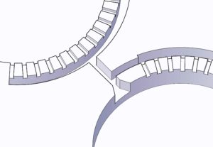
CAD drawing of a multi layer design

Figure 5: SU8 master fabricated with edge bead

Figure 6: SU8 master fabricated without edge bead

Video 1:

Video 2:

References


[1] ‪ Shaurya Prakash, Junghoon Yeom, Nanofluidics and Microfluidics: Systems and Applications ‪Micro and Nano Technologies‪, William Andrew, 2014

[2] Robert D. Deegan, Olgica Bakajin, Todd F. Dupont, Greb Huber, Sidney R. Nagel and Thomas A. Witten, Capillary flow as the cause of ring stains from dried liquid drops, Nature 389, 827-829 (23 October 1997), doi :10.1038/39827

[3] http://www.cns.fas.harvard.edu/facilities/docs/SOP031_r2_6_SU-8%20photolithography%20process.pdf

Digg This
Reddit This
Stumble Now!
Share on Facebook
Bookmark this on Delicious
Share on LinkedIn
Bookmark this on Technorati
Post on Twitter
Google Buzz (aka. Google Reader)

A simple and low cost method to fabricate NOA microfluidic chips

Gabriele Pitingolo1, Raffaele Vecchione1,3 and Paolo A. Netti1,2,3

1 Center for Advanced Biomaterials for Healthcare, Istituto Italiano di tecnologia (IIT@CRIB), Largo Barsanti e Matteucci, 53, 80125, Naples, Italy.

2 Dipartimento di Ingegneria Chimica, dei Materiali e della Produzione Industriale D.I.C.MA.P.I, Università di  Napoli  Federico II, Naples 80125, Italy.

3 Centro di Ricerca Interdipartimentale sui Biomateriali (CRIB), Università di Napoli Federico II, p.le Tecchio 80, Naples, 80125, Italy

Why is this useful?


Microfluidic chips are often made of silicon or glass which presents the drawbacks of being relatively expensive, time consuming and has limitations to the geometries that can be realized. PMMA is an optimal solution to overcome these aspects but it presents a low chemical resistance to organic solvents and aggressive chemicals

Norland Optical Adhesive 60 (“NOA60”) is a clear, colorless, liquid photopolymer that cures when exposed to ultraviolet light1. Surface bonding can be activated with light therefore monolithic and transparent devices especially useful for optical elements can be realized. In particular, the use of NOA 60 eliminates premixing, drying, or heat curing operations common to other optical adhesive systems. Curing time is a matter of minutes and is dependent upon the thickness applied and the energy of ultraviolet light available. Dupont and colleagues have recently developed a NOA microfluidic channel via a photolithography multistep method that presents a long time process2.

Here, we demonstrate the possibility to micromachine already cured NOA substrates by micromilling that is much easier and cheaper than photolithographic techniques for fabrication of microchannels or microstructures in general.  In addition, by micromilling it is possible to easily drill and make open channels in NOA substrates if needed. Also, in the case of microstructures on the two layers to be bonded if one layer presents microstructures with feature sizes below 25 micron and one substrate with feature sizes above this value then it is possible to prepare one substrate by photolithographic techniques and the other substrate by micromilling with following bonding, saving time and money.

What do I need?


  • Fully cured PDMS mold
  • Norland Optical Adhesive 60
  • UV light (E-Series Ultraviolet Hand Lamps)
  • Micromachining machine
  • Oxygen plasma machine
  • Clamp

What do I do?


1. Pour liquid photopolymer NOA into a preformed PDMS mold covering the entire surface (figure 1A). After a few minutes to stabilize the liquid polymer put the PDMS mold under UV light for 30 minutes at a  365 nm wavelength (fig.1B).

2. After the curing time, NOA substrate is ready to use; to fabricate a microfluidic chip two NOA substrates are prepared. NOA substrates are replicated onto flat PDMS surfaces exploiting the flexibility of the PDMS mold as shown in figures 2A and 2B.

3. Take the NOA substrate and mill a channel and related inlet/outlet holes using a micromilling machine (Minitech CNC Mini-Mill) (fig. 3A-3B), the certified positioning accuracy of the three-axis are 12″ / 300mm in x-axis, 9″ / 228mm in y-axis, and 9″ / 228mm in z-axis. To minimize the experimental uncertainty, the NOA substrates preformed in point 2 are smoothed before milling.

4. Prepare the NOA channel (clean with water and dry with an absorbent cloth) and  treat the channel and top layer by exposing to oxygen plasma for 60s, at a pressure less than 0.1 Torr and with a plasma power of 20 W (fig 4A). Clamp the two substrates and put the clamped channel under UV-light for 1 h finalizes the bonding process (fig 4B).

5. Your well-bonded NOA microfluidic chip (Figure 5) is now ready to use.


References

  1. https://www.norlandprod.com/literature/60tds.pdf
  2. E. P. Dupont, R. Luisier and M. A. M. Gijs, Microelectronic Engineering, 2010, 87, 1253-1255.
Digg This
Reddit This
Stumble Now!
Share on Facebook
Bookmark this on Delicious
Share on LinkedIn
Bookmark this on Technorati
Post on Twitter
Google Buzz (aka. Google Reader)

The use of polymer filaments or metal wires to pattern arbitrary-shaped micro-sized electrodes for microfluidic applications

Bruno Rafael Becker1, 2, Tristan Sun1, Shengjie Zhai1 and Hui Zhao1

1. Department of Mechanical Engineering, University of Nevada, Las Vegas NV, US

2. Department of Mechanical Engineering, Universidade Tecnologica Federal do Parana, Brazil

Why is this useful?


Electric fields are widely used to manipulate particles or fluid in lab-on-a-chip systems, for example to separate or assemble particles and pump or mix liquids, due to their favorable scaling with miniaturization. In order to exploit the advantages of electric fields, electrodes have to be fabricated and integrated with lab-on-a-chip devices. Patterned electrodes can also serve as biosensing by measuring the electric current change due to biomolecular binding. Traditional lithography has been used for such electrode fabrication, but particularly for arbitrary shaped electrodes, it is time consuming, requires expensive equipment and needs to be conducted in a cleanroom environment.

Hence, here we developed a simple fabrication method using commercial polymer fishing lines or metal bonding wires as a mask that does not require sophisticated procedures, expensive specialized instruments, and can be done outside a cleanroom environment. The gap size between the electrodes can be controlled by the commercial polymer fishing lines or metal bonding wires (from 1 mm to 1 mm). Due to the flexibility of fishing lines or metal wires, electrodes with arbitrary shapes can be readily fabricated by manipulating flexible lines. The fabrication method is particularly useful for demonstration of proof-of-concept or quick prototyping in terms of searching for the optimal shape, or researchers who lack the access to cleanroom or expensive lithographic equipment.

What do I need?


  • Glass slides
  • 3M double-sided tape
  • Deionized water (DI water)
  • Isopropyl alcohol
  • Acetone
  • Ultrasonic cleaner
  • Plasma cleaner
  • Sputter coating machine
  • Commercial fishing lines or metal bonding wires

What do I do?


1. Use DI water to clean the glass slide in the ultrasonic cleaner for 240 seconds and then dry the slide with the pressurized air (Fig. 1).


Fig 1. Using the ultrasonic cleaner to clean the glass slide.

2. Repeat the step 1 with isopropyl alcohol.

3. Repeat the step 1 with acetone. Acetone not only dissolves remaining contaminants but also provides negative surface charges to the glass surface to prevent adhesion of colloidal particles.

4. Put the glass slide into the oxygen plasma cleaner for 2 minutes (Fig. 2).

Fig 2. Using the plasma cleaner to clean the glass slide.

5. Use the double-sided tape to fix the fishing line on the glass slide.

6. Cover the glass slide with a cut paper. The cut paper along with the fishing line serves as a mask. The double-sided tape also keeps the paper fixed on the glass slide (Fig. 3).

Fig 3. The fishing line along with the cut paper serves as the mask.


7. Place the glass slide covered with the mask in the sputter coating machine (Fig. 4).

Fig 4. Put the glass slide into the sputter coating machine.

8. Sputter coating for 50-60 seconds to get 50-60 nm thickness metal electrodes.

9. Remove the mask from the glass slide (Fig. 5).

Fig 5. Patterned electrodes with the fishing line ready for use.

What else should I know?


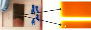
Copper wires with a diameter of 140 µm were also tested. But because of their rigidity, they could not be aligned securely with the glass surface; consequently, the gold was sputtered around the wire and contaminated the channel. A 25 µm gold bonding wire was tested to determine the applicability of the method to fabrication with even smaller feature sizes. Electrodes with a 25 µm gap size are successfully fabricated, showing the robustness of our method (Fig. 6).


Fig 6. Patterned electrodes with the 25 µm gold bonding wire.

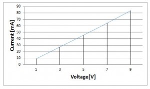
In the end, we connected the electrodes with a 100 ohms resistor with the electrodes, applied a voltage, measured the current, and plotted the I-V curve (Fig. 7). The I-V curve shows that the resistance of the electrodes is around 10 ohms, demonstrating the effectiveness of our method in patterning electrodes.

Fig7. Measured currents as a function of the applied voltages.

Experiments with the fabricated gold electrodes


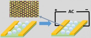
We used the fabricated electrodes to assemble colloidal particles into functional structures (Fig. 8). Due to the dipole-dipole interactions induced by the applied electric fields, 5 micrometer latex particles are assembled into ordered structures with an AC electric field of 100 KHz and 10 V, which can find applications in photonics or biosensing.


Fig.8 Assembly of 5 m colloidal particles using the electric field.

Digg This
Reddit This
Stumble Now!
Share on Facebook
Bookmark this on Delicious
Share on LinkedIn
Bookmark this on Technorati
Post on Twitter
Google Buzz (aka. Google Reader)

Different strategies for the fabrication of cell culture chambers for live-cell imaging studies

David Caballero1,2, Josep Samitier1,2

1 Nanobioengineering group, Institute for Bioengineering of Catalonia (IBEC), Barcelona, Spain

2 Centro de Investigación Biomédica en Red de Bioingeniería, Biomateriales y Nanomedicina (CIBER-BBN), Zaragoza, Spain.

Why is this useful?


Long-term imaging of cells is typically performed using standard Petri dishes. Frequently, these ´chambers´ are not convenient when sample manipulation and treatment (e.g. functionalization, immunostaining…) is needed, both before and after the experiment1. To overcome this ´problem´, glass coverslips are used. They can be easily manipulated when following multistep protocols prior to cell deposition. For live-cell microscope imaging, the customized coverslips are secured into holders (chambers) containing the adequate cell culture medium2, 3. These holders are either supplied by the microscope manufacturers or fabricated in a mechanical workshop; this implies time for the design and money.

In this work we show two different strategies for the simple, fast and cheap fabrication of chambers for live-cell imaging, using materials and simple tools typically available in a bioengineering laboratory. These materials include Petri dishes, polydymethylsiloxane (PDMS), Falcon tube cap and glass coverslips. In the first strategy (A) we drill a hole in a Petri dish where a customized glass coverslip is adhered at the bottom using wax. In the second strategy (B), a PDMS frame is used to hold the coverslip inside a Petri dish. Depending on the user final application one strategy is recommended over the other (see below). All the material is biocompatible and simple to obtain. These two methods provide several advantages: (i) they are easy and cheap; (ii) the chambers can be fabricated in a short-time period; (iii) this approach avoids the purchase of commercially-available holders or ordering the fabrication to a mechanical workshop.

What do I need?


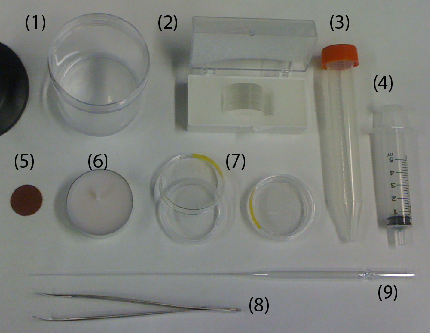
    Figure 1

Figure 1. Material needed for the fabrication of the home-made chambers.

(1) PDMS
(2) Glass coverslip #1, 25 mm in diameter
(3) Cap of a 15 mL Falcon (any brand)
(4) Syringe 5mL
(5) Polishing paper
(6) Wax
(7) P35 plastic Petri dish (any brand)
(8) Sharp Tweezers
(9)Glass Pasteur pipette

You will also need:

  • Hot plate
  • Bunsen burner (optional)
  • Soldering iron (or drill)
  • EtOH 70%
  • Oven
  • SYLGARD 184 PDMS and crosslinker agent (Dow Corning)


What do I do?


Figure 1 (above) shows all the material needed for the fabrication of the home-made chambers using both strategies A and B. The steps describing both strategies are detailed next.

STRATEGY A:

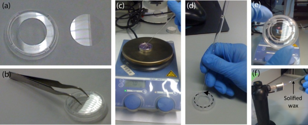
1. Make a circular hole of around 2 cm in diameter in the middle of the lower part of a P35 Petri dish using a pre-heated, sharp-tip soldering iron. Alternatively, a drill can be used. Ensure a perfect circular hole by using a 15 mL Falcon cap as a template (see Fig.2a-c).

Figure 2. Fabrication of the cell culture chamber using Strategy A. Drilling a hole on the lower part of a Petri. (a) First, draw a circumference of about 2 cm in diameter in the center of the lower part of a Petri dish. Use a 15 mL Falcon cap as template. (b-c) Next, a soldering iron is used to drill a hole. (d) Finally, the edge of the hole is polished using thin polishing paper.

2. Polish the hole using polishing paper (see Fig.2d). Check that the Petri is free of debris. Rinse the sample with etOH 70%. (Optional: Sonicate).

3. Use the tweezers to place and secure the glass coverslip on the back side of the holey dish with its customized side (e.g. functionalized) facing the inner part of the Petri (see Fig.3a-b).

Figure 3. Adhering the glass coverslip to the lower part of the drilled Petri dish using wax. (a) The drilled Petri dish and glass coverslip #1, 25 mm in diameter are (b) placed together and secured using the tweezers. (c) Next, the wax is melted using a heat plate. A small volume is absorbed by capillarity using a glass Pasteur pipette. (d) Following the edge defined by the coverslip and the dish, the chamber is sealed. This step is critical to ensure a good sealing. (e) Check that no open remaining points are left. (f) A Bunsen burner or equivalent can be used to melt the solidified wax inside the pipette.

4. Melt the wax using the hot plate and fill the Pasteur pipette with a small volume (see Fig.3c). NOTE: Capillarity will make the liquid wax to flow inside the pipette.

5. Gently, put in contact the tip of the pipette (filled with wax) with the coverslip. Follow the edge formed by the coverslip and the Petri (see Fig.3d). Cover it completely with wax until the entire contour is sealed (see Fig.3e). Refill the pipette if necessary. NOTE 1: The wax may solidify inside the pipette quickly. If so, melt it again using the Bunsen burner (or equivalent) (see Fig.3f). NOTE 2: Ensure that no empty spaces are left; cell medium will flow through them.

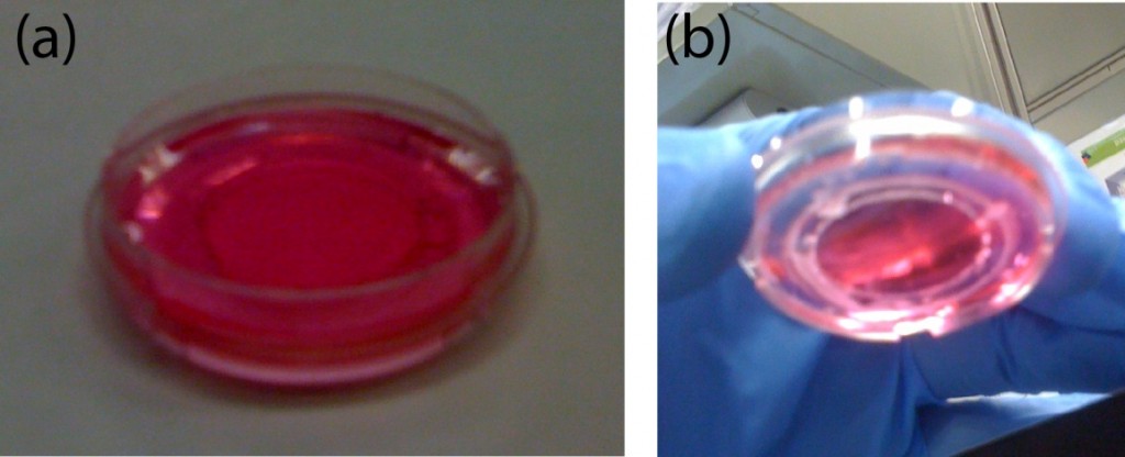
6. Culture the cells of interest (see Fig.4). Place the chamber inside the microscope and start the live-cell imaging experiment. NOTE: Manipulate gently the sample.

Figure 4. Finished chamber for live-cell imaging experiments. (a) Front view of the chamber filled with cell culture medium. (b) Back side view showing the wax-sealed region. No leakage is observed. The coverslip can be easily recovered after the experiment by pushing it down gently with the tweezers.

7. At the end of the experiment, the medium can be removed and the coverslip detached by pushing it down gently with the tweezers. Treat the sample as desired (e.g. immunostaining).

STRATEGY B:

1. Insert upside down the cap of a 15 mL Falcon in the middle of a P35 Petri dish (see Fig.5a).

Figure 5. Fabrication of the cell culture chamber using Strategy B. (a) A 15 mL Falcon cap is placed in the center of a P35 Petri dish. The empty region is filled with PDMS using a syringe. (b) The sample is degassed and cured. (c) The cap is removed and the PDMS frame released.

2. Fill the empty space with a syringe (or equivalent) with PDMS in a 10:1 ratio (pre-polymer:cross-linker). Degass and cure it at 65ºC for 4h (see Fig. 5b). NOTE 1: Holding the cap with adhesive tape will ensure that it remains in the center during curing. In this case, curing must be performed at RT overnight. NOTE 2: A very thin PDMS layer may appear after the removal of the cap. Remove it manually to ensure a through-hole in the PDMS. Alternatively, a weight can be applied on top of the cap.

3. Remove the cap using the tweezers and release the PDMS frame (see Fig. 5c).

4. Sterilize the PDMS frame. Rinse it with etOH 70% and UV-irradiate for 15 min.

5. Working in the cell culture room, deposit a drop (~50 uL) of culture medium in the center of a new P35 Petri dish (see Fig. 6a).

Figure 6. Finished chamber for live-cell imaging experiments. (a) A small drop of cell culture medium is deposited in the center of a new P35 Petri dish. (b) The customized coverslip is placed on top of it. (c) The PDMS frame is introduced inside the Petri and pushed down to hold the coverslip forming the chamber. Finally, the chamber is filled with cells.

6. Place the (customized) glass coverslip facing-up on top of the drop (see Fig. 6b). NOTE: This will ensure that no air bubbles are formed. Hold it with the PDMS frame.

7. Culture the cells of interest (see Fig. 6c). Place the sample inside the microscope and start the experiment.

8. At the end of the experiment, the medium can be removed and the coverslip released by removing the PDMS frame with the tweezers. Treat the sample as desired (e.g. immunostaining).

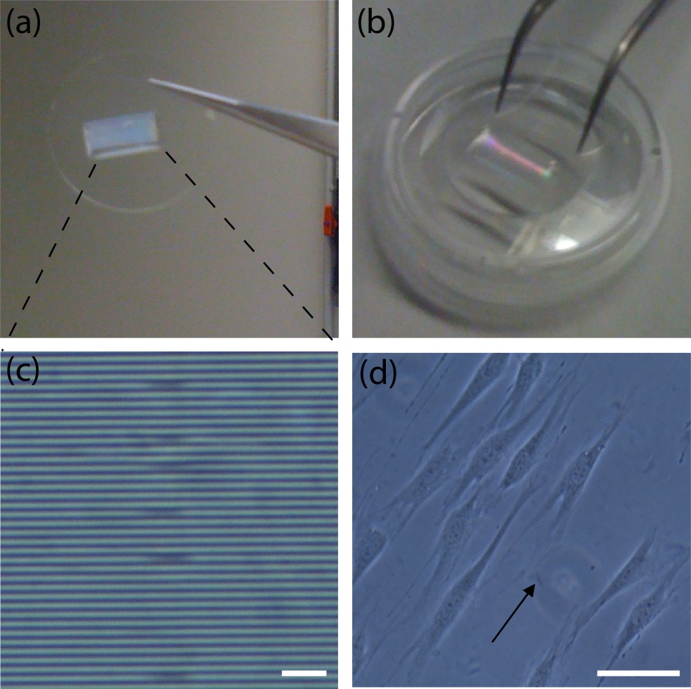
Figure 7. Microfabricated coverslips for live-cell imaging studies. (a) Glass coverslip covered with PDMS microstructures. (b) The modified coverslip can be used for the fabrication of chambers using both strategies. (c) Zoomed image of the microstructures (parallel grooves). The dimensions are: 1 um x 1 um x 1 cm (HxWxL); the separation between grooves is 1 um. Scale bar: 10 um. (d) NIH3T3 fibroblasts aligned parallel to the grooves. The arrow shows the direction of the structures. Scale bar: 50 um.


What else should I know?


By using these two approaches, chambers can be easily fabricated in the lab. Most importantly, this approach allows the manipulation of coverslips before and after the experiment with cells. If the coverslips are (bio)chemically modified (e.g. micropatterned with proteins of the extracellular matrix), manipulation must be performed carefully and fast to avoid sample degradation. Similarly, for cell guidance assays, coverslips can be easily modified with microfabricated structures to orient cell growth and motility (see Fig. 7), following the same steps described in this protocol.

For Strategy A, users must be aware of the melting temperature of wax (around 45ºC). This implies that the sealing may be fragile when performing the experiments at 37ºC and manipulation must be performed gently to avoid liquid leakage. Other materials and shapes, besides circular glass coverslips, could be used. This will depend on the experimental requirements of the user. For Strategy B, the PDMS frame and the coverslip could be used without the Petri in some applications. However, for live-cell imaging, a perfect fit between the chamber and the microscope stage is needed and the use of the Petri is therefore strongly recommended.

Finally, the user must consider the magnification needed for the experiment and the thickness of the sample on each strategy. Strategy A is recommended for high magnification microscopy (40X – 100X) and Strategy B for low magnification (4X – 20X). If needed, thinner coverslips (#0) could be used.


Acknowledgements

Dr. Daniel Riveline, Dr. Jordi Comelles (Laboratory of Cell Physics ISIS/IGBMC, Strasbourg, France) and David Izquierdo (Nanobioengineering group – IBEC, Barcelona, Spain) are acknowledged for technical help and discussions.

References

1.      Zanella F, Lorens JB, Link W. High content screening: seeing is believing. Trends Biotech 2010; 28:237-45.

2.      Caballero D, Voituriez R, Riveline D. Protrusion Fluctuations Direct Cell Motion. Biophysical Journal 2014; 107:34-42.

3.      Riveline D, Buguin A. Devices and methods for observing the cell division WO/2010/092116, 2009.

Digg This
Reddit This
Stumble Now!
Share on Facebook
Bookmark this on Delicious
Share on LinkedIn
Bookmark this on Technorati
Post on Twitter
Google Buzz (aka. Google Reader)

Reservoir Poly(dimethylsiloxane) Cap Fabrication

Luis G. Rigat-Brugarolas1,2, Antoni Homs-Corbera1,2 and Josep Samitier1,2,3

1 Nanobioengineering group, Institute for Bioengineering of Catalonia (IBEC), Barcelona, Spain
2 Centro de Investigación Biomédica en Red de Bioingeniería, Biomateriales y Nanomedicina (CIBER-BBN), Zaragoza, Spain.
3 Department of Electronics, Barcelona University (UB), Martí I Franques, 1, Barcelona, 08028, Spain.

Why is this useful?


Microfluidic devices are often connected to external reservoirs in order to perform experiments with large samples or to generate some types of closed loop systems.1 When containing biological content, once sealed and fluidically connected, these reservoirs should allow proper gas exchange and facilitate their placement in a controlled environment such as an incubator.2 On the other hand, often the connections used for this kind of assays may also suffer from sample leakages.

In this work we present a simple and cheap way of facing these issues by introducing a fabrication methodology for a sealing cap made of poly(dimethylsiloxane) (PDMS) that can be used for any kind of reservoir or bottle. The cap can be customized in order to allow multiple tubing connections depending on the specific user needs. PDMS is easy to manipulate, it’s biocompatible and permits gas exchange.3 This solution, consisting on fabricating a flexible PDMS cap covering the reservoir, should become a versatile alternative to expensive or unreliable other strategies and could be used in several microfluidic applications.

What do I need?


  • PDMS and crosslinker agent.
  • Plastic or glass reservoir.
  • Scalpel.
  • Tubing.
  • Oven.
  • Harris Uni-Core punchers or any kind of punchers.
  • Petri dishes.
  • Plasma cleaner.

What do I do?


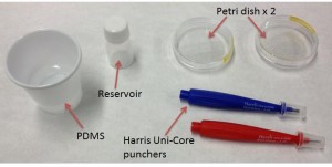
Figure 1 shows the basic utensils and products needed to fabricate the PDMS cap.


Fig 1: Basic utensils and products needed to fabricate the PDMS cap

The steps are detailed next:

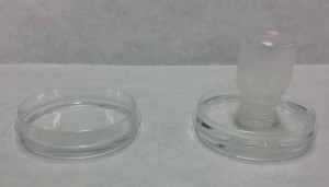
  1. Place reservoir/bottle in an upside down position inside a Petri dish. Fill the plate with PDMS as shown in Figure 2. In addition, fill another empty Petri dish with a thin layer of PDMS.
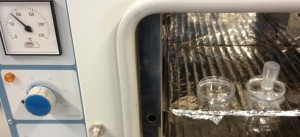
  2. Place both plates/samples inside an oven in a 65-90 ºC temperature range (depending on the reservoir’s material) for about 1.5 hours (Figure 3).
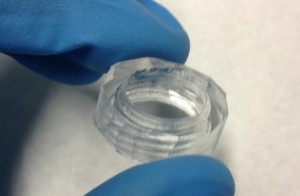
  3. Once the samples have polymerized, they have to be taken from the dishes (Figure 4), and the one corresponding to the reservoir cap replica can be cut, if needed, with a scalpel, as shown in Figure 5.
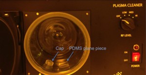
  4. After cleaning both samples with ethanol, they have to be chemically modified in O2 plasma (1 minute at high frequency, Figure 6) and immediately pressed together to form a permanent bond. It is important that the flat piece is sealed to the correct side of the cap replica.
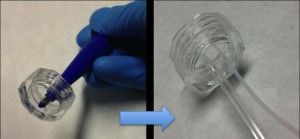
  5. Once the final piece is achieved (Figure 7 left), it is useful to use Harris Uni-Core punchers in order to pierce the sample with the diameter of the tubing that is going to be used. It is recommended to make the holes with a slighter smaller diameter than the outer diameter of the tubing to form a pressure seal between the tubing and the hole (Figure 7 right); this will prevent leakage of the sample or undesired particles entering to the reservoir.
  6. Finally it is possible to screw the PDMS cap into the reservoir (an example is shown in Figure 8).

Fig 2: Fill two Petri dishes with PDMS, one with the reservoir (upside down) and the other just has to be covered with a thin polymer layer

Fig 3: Dispose the dishes inside an oven for 1-2 hours at 65-90ºC

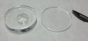
Fig 4: An example of two PDMS samples. The left one corresponds to the reservoir cap replica. The right one to the PDMS thin layer

Fig 5: PDMS cap replica

Fig 6: Dispose both samples in a plasma cleaner in order to chemically modify the PDMS surfaces and join the cap with the PDMS plane piece

Fig 7: In order to pierce the access holes, a puncher is needed; afterwards the tubing can be connected to the PDMS cap

Fig 8: Example of a PDMS cap screwed into a plastic reservoir


References

[1] Herricks T., Seydel KB., Turner G., Molyneux M., Heyderman TT., Rathod PK.  (2011) A microfluidic system to study cytoadhesion of Plasmodium falciparum infected erythrocytes to primary brain microvascularendothelial cells. Lab Chip, 11, 2994.

[2] Rochow N., Manan A., Wi W., Fusch G., Monkman S., Leung J., Chan E., Nagpal D., Predescu D., Brash J., Selvaganapathy PR., Fusch C. (2014) An integrated array of microfluidic oxygenators as a neonatal lung assist device: in vitro characterization and in vivo demostration. Artif Organs, Doi: 10.1111/aor.12269.

[3] Regehr KJ., Domenech M., Koepsel JT., Carver KC., Ellison-Zelski SJ., Murphy WL., Schuler L., Alarid ET., Beebe DJ. (2009) Biomedical implications of polydimethylsiloxane-based microfluidic cell culture. Lab Chip, 9, 2132–2139.

Digg This
Reddit This
Stumble Now!
Share on Facebook
Bookmark this on Delicious
Share on LinkedIn
Bookmark this on Technorati
Post on Twitter
Google Buzz (aka. Google Reader)

Simple fabrication of three-dimensional ramped microstructures using SU-8 negative photoresist

Luis G. Rigat-Brugarolas1,2, Antoni Homs-Corbera1,2 and Josep Samitier1,2,3

1 Nanobioengineering group, Institute for Bioengineering of Catalonia (IBEC), Barcelona, Spain 2 Centro de Investigación Biomédica en Red de Bioingeniería, Biomateriales y Nanomedicina (CIBER-BBN), Zaragoza, Spain.

3 Department of Electronics, Barcelona University (UB), Martí I Franques, 1, Barcelona, 08028, Spain.

Why is this useful?


At present, normal photolithographic techniques constitutes binary image transfer methodologies, where the developed pattern consists of regions with or without photoresist depending whether the UV Light has been in contact with the sample or not during the exposure process.1 Complex 3D patterns construction is of increasing importance in the miniaturization of fluidic devices.2 In the following work we introduce a photoresist-based technique to produce three-dimensional ramped microstructures for lab-on-a-chip applications.

We present a new technique that can be used to form multilevel features in SU-8 or any other negative photoresist using a single photolitograpy step, thus minimizing stages in the fabrication process in a simple and cheap way. This method thereby allows using a normal photomask without needing to add a complementary grayscale pattern, enabling complex microchannel structures.

What do I need?


  • Common items and devices used in photolitographic processes (mask aligner, hot plates, chemical baths, negative photoresist and transparent substrate)
  • Step Variable Metallic Neutral Density Filters (Thorlabs, Inc., NJ, USA).

What do I do?


  1. Dispose the sample in the mask aligner with the SU-8 photoresist on the bottom side as depicted in Figure 1. This will force UV light to cross through the transparent substrate and to first polymerize those photoresist regions in contact with the substrate.
  2. Place the photomask in the aligner standard position, normal to the light beam.
  3. Select the filter (continuous, step, etc.) according to your needs (see an example in Figure 2).
  4. Place the filter in the position between the photomask and the UV light source, with the filter’s design in contact with the photomask (see Figure 3).
  5. Enter a correct UV exposure time; since another element is going to be added in the UV light trajectory, this value has to be adjusted (final result in Figure 4).

Fig 1: Scheme of disposal of the SU-8 photoresist in the mask aligner for achieving relief structures.

Fig 2: Example of rectangular step filter available at Thorlabs, Inc.

Fig 3: Step filter placed between the photomask and the UV light source.

Fig 4: Example of three-dimensional ramped structure constructed using SU-8. Relief characterization obtained with a profilometer. The white line represents the structure obtained after the development process (with an angle value of 30º), showing a slope from 0 µm to 12 µm (in this case, a rectangular step filter was used). The red line shows what it would look like the profile if no filter had been dispose between the photomask and the UV light source.

What else should I know?


As with any negative photoresist, grayscale exposure in conventional processes will lead to hardening the surface, removing the substrate if unattached during the development, in a methodology normally used to create cantilever structures. This is why it is important, when trying to create relief structures, to turn the sample and expose it from the glass substrate side leaving the SU-8 or any other negative photoresist on the bottom side.

Acknowledgments


We thank David Izquierdo and Juan Pablo Agusil for their technical help and for providing the material.


Reference

[1] S.D. Minteer. Microfluidic techniques: reviews and protocols. Humana Press, 2006. ISSN: 1064-3745.

[2] C. Chen, D. Hirdes, A. Folch. Gray-scale photolithography using microfluidic photomasks. PNAS, 2003. DOI:10.1073

Digg This
Reddit This
Stumble Now!
Share on Facebook
Bookmark this on Delicious
Share on LinkedIn
Bookmark this on Technorati
Post on Twitter
Google Buzz (aka. Google Reader)