Author Archive

Cutting the cords: Two paths to well-plate microfluidics

Sara E. Parker1 and Peter G. Shankles2, Maddie Evans1, Scott T. Retterer1,2,3

1 Biosciences Division, Oak Ridge National Laboratory, Oak Ridge, TN

2 The Bredesen Center, The University of Tennessee, Knoxville, TN

3 The Center for Nanophase Materials Sciences

Why is this useful?

Even simple microfluidic devices often require complex and expensive pumping and valving systems for accurately metering and controlling fluid flow. This often necessitates substantial and time-consuming set-up, and sometimes make these chips unwieldly and difficult to image. It can also represent a significant departure from the rather straight forward process of pipetting fluids from one small volume to another, making adoption by non-microfluidic experts unlikely. However, the development of well-plate microfluidics1,2 provides a high throughput, simplified method for studying fluid exchange and shear flow, while minimizing the set-up and need for multiple fluid connections. Creating an interface between the polystyrene (PS) plate and the polydimethylsiloxane (PDMS) fluidics presents the largest obstacle in creating these hybrid devices. Khine et al.1 utilized pressure to create a tight interface while Conant et al.2 adhered the surfaces using glue, but neither elaborated on their techniques and in practice small changes in the process can result in failed devices. Here, two techniques are detailed on consistently creating an effective interface between the well-plate and microfluidics. Resulting in individual wells that are interconnected via custom microchannels in a PDMS device attached to the bottom of the well-plate. Reagents are then added to wells and, driven through the underlying channel network into an outlet well via hydrostatic pressure or a pressure control system3,4.

With the use of this platform, flow can be introduced into traditional well-plate studies allowing various physiological conditions to be more closely mimicked. Further, the compatibility of these custom devices with well-plate microfluidic control systems provides the opportunity to precisely and dynamically control experimental conditions including temperature, pressure, and gas environment3,4. The use of multi-well plates also allows for multiple devices to be bonded in parallel to the same plate, increasing throughput without increasing the complexity of the control system5. Additionally, the familiarity and ubiquity of the well-plate platform provides a familiar platform for technical professionals within the lab and is automatically compatible with the host of microscope stage attachments already available for use with conventional well-plates.

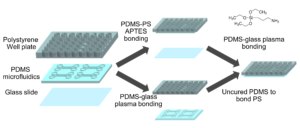
Well-plate microfluidic fabrication has been shown with a pressure seal between the microfluidics and well-plate1 as well as gluing the two together2. This work builds off these ideas by detailing bonding with a liquid adhesive or chemical activation and bonding. The process of bonding customized PDMS devices to well-plates for well-plate microfluidics has only been vaguely described previously5,6. Herein, we present two approaches that utilize either (3-Aminopropyl)triethoxysilane (ATPES) to modify the surface of the PS well-plate to bond with plasma treated PDMS, or uncured PDMS to act as a glue between the PS and PDMS surfaces7. While the APTES modification provides a stronger bond without adding additional material, the uncured PDMS bonding procedure requires less pressure, avoiding any distortion of nanoscale features. An overview of the process is shown in Figure 1:

Figure 1 – Diagram of the fabrication process with the APTES process above and PDMS glue below.

What do I need?

Materials

  • PDMS device replica with inlets and outlets designed to align with a well-plate
  • 48 well-plate; Flat-bottomed, non-tissue culture treated
  • Isopropyl alcohol (IPA)
  • Coverslip or slide large enough to cover channels
  • X-Acto knife
  • Scotch tape

APTES bonding only

  • APTES
  • Deionized water
  • Hard rubber brayer
  • Sealable plastic container

PDMS bonding only

  • Tapered tip plastic syringe (Nichiryo 6mL syringe with tips)
  • Uncured PDMS (10:1 w/w elastomer base to curing agent)

Equipment

  • Drill press
  • Plasma cleaner (Harrick Plasma, Basic plasma cleaner PDC-32G)
  • Hot plate
  • Oven (75°C)

What do I do?

Well-plate preparation (for both bonding methods)

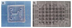
  1. Prepare the well-plate by drilling a hole in the center of each well corresponding to an inlet or outlet on the PDMS replica (Figure 2).
  2. Using an X-Acto knife, clean the edges of the drilled holes such that the bottom surface of the well-plate is smooth and any lips that may have formed from drilling have been removed.

Figure 2 – The prepared PDMS device is shown in a. and the prepared well-plate is shown in b.

APTES bonding Procedure

Well-plate APTES modification

1.      Clean the bottom surface of the well-plate with IPA and expose to oxygen plasma on high setting for 2 minutes, with the bottom surface of the plate facing up (Figure 3a).

2.      In a fume hood, prepare a 100 mL aqueous solution of 1% v/v APTES and pour the solution into a shallow, resealable container.

3.      Place the plasma treated well-plate in the APTES container so that the bottom surface of the plate is completely submerged. Seal the container and let soak for 30 minutes (Figure 3b)

4.      Remove the plate from the APTES bath and rinse the top and bottom with water. Dry the well-plate using compressed air and place it on a 50°C hot plate to ensure thorough drying.
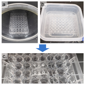
Figure 3 – The well-plate was exposed to air plasma and submerged in a water/APTES solution to modify the surface chemistry and enable bonding between PS and PDMS. A coverslip was then plasma bonded to the PDMS surface.

Assembly

1.      Clean the top of the PDMS replica (opposite to the channels) using scotch tape and plasma clean on high for 1 minute.

2.      With the channeled side of the PDMS replica facing up, align the inlets/outlets of the replica with the holes of the APTES-modified well-plate and press the layers together. Roll a brayer over the surfaces to remove any bubbles and ensure an even, uniform bond. Bake at 75°C for 20 minutes (Figure 3c).

3.      Remove the well-plate with bonded device from the oven and use scotch tape to remove debris from the channel-exposed PDMS. Clean a glass coverslip with IPA and expose the coverslip and well-plate to oxygen plasma on high for 1 minute. Bond the coverslip to the PDMS replica, thus enclosing the channels and bake at 75°C for 20 minutes.

Uncured PDMS procedure

1.      Remove any dust from the bottom (channel-exposed) side of the PDMS replica using Scotch tape and clean a glass coverslip with IPA. Expose both to oxygen plasma for 1 minute on high setting and bond them together, enclosing the channels. Bake at 75°C for 1 hour (Figure 4a).

2.      Clean the bottom surface of the prepared well-plate with IPA. Using the tapered tip syringe, place small droplets of uncured PDMS onto the bottom surface of the well-plate where the PDMS device will be bonded (Figure 4b).

3.      Using scotch tape, remove any dust from the top (opposite to the channels) of the coverslip-bonded PDMS replica. Align the inlets/outlets of the device with the holes of the well-plate and lightly press the device onto the well-plate (Figure 4c). Remove any uncured PDMS that may have leaked into the wells or inlets/outlets of the device. Bake at 75°C for 1 hour.
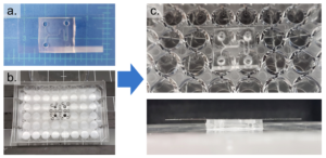
Figure 4 – The PDMS device was first bonded to a coverslip (a) and then bonded to a well-plate using uncured PDMS (b). c shows the completed device from the top and side view.

Conclusion

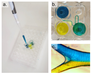
We present two methods for attaching PDMS microfluidic devices to polystyrene well-plates, providing the opportunity to utilize customized channels for well-plate microfluidics. Assays using these devices can be run in conjunction with well-plate microfluidic controllers or using simple pipetting methods by adding the desired reagent or media to the inlet wells (Figure 9). While the fabrication process is more involved than typical PDMS processing, well-plate microfluidics removes the need for complicated tubing connections by working with a single manifold controller, or hydrostatic flow using the well height to produce pressure.

References

1         M. Khine, C. Ionescu-Zanetti, A. Blatz, L. P. Wang and L. P. Lee, Lab Chip, , DOI:10.1039/b614356c.

2         C. G. Conant, M. A. Schwartz, J. E. Beecher, R. C. Rudoff, C. Ionescu-Zanetti and J. T. Nevill, Biotechnol. Bioeng., , DOI:10.1002/bit.23243.

3         Fluxion, White Pap., 2008, 1–6.

4         2012, US00825796.

5         C. G. Conant, J. T. Nevill, M. Schwartz and C. Ionescu-Zanetti, J. Lab. Autom., 2010, 15, 52–57.

6         P. J. Lee, N. Ghorashian, T. A. Gaige and P. J. Hung, J. Lab. Autom., , DOI:10.1016/j.jala.2007.07.001.

7         V. Sunkara, D.-K. Park, H. Hwang, R. Chantiwas, S. a. Soper and Y.-K. Cho, Lab Chip, 2011, 11, 962–965.


Digg This
Reddit This
Stumble Now!
Share on Facebook
Bookmark this on Delicious
Share on LinkedIn
Bookmark this on Technorati
Post on Twitter
Google Buzz (aka. Google Reader)

A second life for old electronic parts: a spin coater for microfluidic applications

Gabriele Pitingolo1, Valerie Taly1 and Claudio Nastruzzi2

1INSERM UMR-S1147, CNRS SNC5014; Paris Descartes University, Paris, France. Equipe labellisée Ligue Nationale contre le cancer.

2Dipartimento di Scienze della Vita e Biotecnologie, Università di Ferrara, Ferrara, Italia

*Email: gabriele.pitingolo@parisdescartes.fr, nas@unife.it

Why is this useful?

It is well known that the rapid proliferation of information and communications technologies (ICT) has resulted in a global mountain of high-tech trash (e-waste). The problem with e-waste is not only the accumulation of electronic products and therefore the high disposal costs, but rather the hazardous substances present in their various components. Therefore, the importance of recycling is evident in the area of resource and energy conservation, finding a new, second life for electronic components.

Spin coaters are widely used instruments useful to deposit uniform thin films to flat substrates [1]. In microfluidics, the spin coating is used to coat a photoresist layer (such as SU-8) or to bond separate substrates by using the adhesive properties of PDMS. The spin coating technology is also used to fabricate thin polymer membranes. PDMS membranes are, for example, employed for a wide range of applications due to their several advantages. For instance, being PDMS membrane permeable, they can be used to exchange gas (in cell culture application for example) or small molecule (in filtration application) [2]. In addition, as recently reported, spin coating is suitable to fabricate microchannels with a circular section [3].

Unfortunately, most commercial spin coaters are expensive (£2,000-6,000) and possess some unwanted or redundant specifications, not necessarily needed for the fabrication/modification of microfluidic devices.

In this respect, we present here a tip to develop portable spin coaters by recycling computer fans and mobile phone wall chargers. The most common fans in personal computers have a size of 80 mm, but the size can range from 40 to 230 mm. It’s also known that the fans of different size show also a different rotational speed. Typically, the 80 mm fans have a rotational speed of 2000 rpm (that represent a suitable speed for common thin layering in microfluidics).

What do I need?

Parts for the spin coater

  • Personal computer fan
  • Insulated male/female wire pin connectors
  • Tesa power strip
  • Wall chargers from (old) mobile phones

Parts and chemicals for the specific examples

  • Milled poly(methyl methacrylate) (PMMA) microchannel
  • Glass slide
  • Sylgard® 184 silicone elastomer kit
  • Clumps

What do I do?

Assembling of spin coater

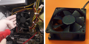
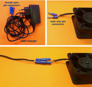
1.Remove the fan from an old pc (or mac, if are particularly posh) (Fig.1).

2. Connect the wall charger and the fan wires with insulated female and male wire pins. Afterwards, to turn on the fan, connect the female and male pins.

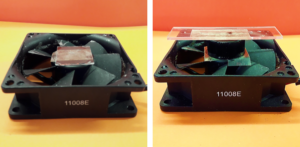
3. Using the tesa power strips, secure the substrate (i.e. glass slide or PMMA microchannel) to the central part of the fan (left picture). For devices larger than the fan, use an adeguate plastic stopper to elevate the device (right picture).

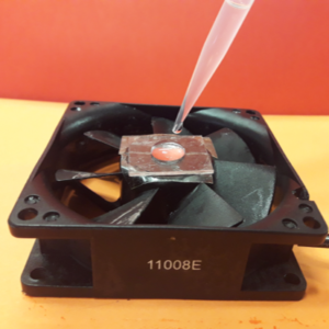
4. Drip, by a (micro)pipette, the liquid containing the coating material on top of the substrate.

5. Turn on the fan and spin coat the substrate for about 30 seconds (time can vary depending on the substrate viscosity and coating thickness required).

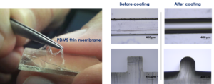
6. Verify the coating by peeling off the PDMS membrane from the glass slide by tweezer (left picture) or analyze the microchannel profile by microscopy (right panels).

What else should I know?

In this tip a portable spin coater for microfluidic applications was developed using old electronic parts. A single fan can be re-used many times (up to hundreds in our experience). The amount of PDMS (in form of droplets) falling on the fan is quite limited. If necessary the fan can be cleaned after any use by simply rubbing it with a wipe soaked with some petroleum ether (aka liquid paraffin or white petroleum). In the worst cases (very rarely occurring) the fan can be easily replaced, since they are available for free by any old unused PC.

Acknowledgements

This work was supported by the Ministère de l’Enseignement Supérieur et de la Recherche, the Université Paris-Descartes, the Centre National de la Recherche Scientifique (CNRS), the Institut National de la Santé et de la Recherche Médicale (INSERM). This work was founded by CAMPUS FRANCE (n° 39525QJ) and carried out with the support of the Pierre-Gilles de Gennes Institute equipment (“Investissements d’Avenir” program, reference: ANR 10-NANO 0207). Financial support from the Università italo-francese grant G18-208 is gratefully acknowledged.

References

[1]          D. B. Hall, P. Underhill, and J. M. Torkelson, “Spin coating of thin and ultrathin polymer films,” Polymer Engineering & Science, vol. 38, no. 12, pp. 2039-2045, 1998.

[2]          S. Halldorsson, E. Lucumi, R. Gómez-Sjöberg, and R. M. Fleming, “Advantages and challenges of microfluidic cell culture in polydimethylsiloxane devices,” Biosensors and Bioelectronics, vol. 63, pp. 218-231, 2015.

[3]          R. Vecchione, G. Pitingolo, D. Guarnieri, A. P. Falanga, and P. A. Netti, “From square to circular polymeric microchannels by spin coating technology: a low cost platform for endothelial cell culture,” Biofabrication, vol. 8, no. 2, pp. 025005-025005, 2016 May 2016.

Digg This
Reddit This
Stumble Now!
Share on Facebook
Bookmark this on Delicious
Share on LinkedIn
Bookmark this on Technorati
Post on Twitter
Google Buzz (aka. Google Reader)

Development of a cell culture microdevice with a detachable channel for clear observation

Eriko Kamata, Momoko Maeda, Kanako Yanagisawa, Kae Sato*

Department of Chemical and Biological Sciences, Faculty of Science, Japan Women’s University, Bunkyo, Tokyo 112-8681, Japan

*E-mail: satouk@fc.jwu.ac.jp

Why is this useful?

There have been many reports on microfluidic devices for cell culture having upper and lower microchannels separated by a thin PDMS membrane. In these devices, the lower channel often interferes with the microscopic observation of cells cultured in the upper channel. To avoid interference, a microdevice with a detachable lower channel was developed.

What do I need?

Materials:

PDMS (SILPOT 184w/c, Dow Corning Toray)

Hexane

PMMA sheet (56 × 76 × 2 mm)

Glass slides (52 × 76 mm and 26 × 76 mm)

Cover slip (24 × 60 mm)

1 kg weight

PTFE tubing (1 × 2 mm and 0.46 × 0.92 mm)

Tygon tubing (1.59 × 3.18 mm)

Biopsy Punches (1 mm and 2 mm, Kai corporation)

Equipment:

Vacuum desiccator

Oven (65 ˚C and 100˚C)

Spin coater

Plasma generator

Vacuum pump

What do I do?

  1. PDMS molding

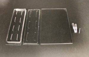
Mix the elastomer and curing agent at a 10:1 mass ratio. De-gas the mixture under vacuum until no bubbles remain (20 min). Pour the degassed PDMS mixture onto a master, which has an upper channel (1 × 1 × 10 mm) or a lower channel (0.5 × 2 × 15 mm) structure, and then place it in an oven at 65˚C for 1 h. Peel off the PDMS replica from the master and adhere it to a glass slide (26 × 76 mm). Place it in an oven at 100˚C for 1 h (Fig.1).

  1. Preparation of a thin PDMS membrane

Spin coat 600 µL of the PDMS prepolymer (at a 10:1 mass ratio) on a PMMA sheet at 500 rpm for 20 s followed by 2,400 rpm for 600 s. Bake it at 65˚C for 1.5 h.

Fig.1 PDMS sheet with the upper channel, that with the lower channel, PDMS membrane, and tubing.

  1. Permanent bonding of the PDMS membrane and the sheet with the upper channel

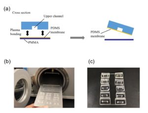
Punch the inlet and outlet holes at both the ends of the upper channel with a 2-mm biopsy punch. Expose both the bonding surfaces of the PDMS membrane and the PDMS sheet with the upper channel (upper sheet) to plasma at 100 W, 35 s (Fig.2a and 2b). Laminate and bake them at 65˚C for 1 h (Fig.2c). Remove the PMMA sheet, and punch a hole to connect the sheet with the lower channel by using a 1-mm biopsy punch from the membrane side.


Fig.2 (a) Schematic diagram of bonding the PDMS membrane and the upper sheet. (b) Plasma treatment. (c) Bonded PDMS membrane and sheet.

  1. Detachable bonding of the PDMS membrane and the PDMS sheet with the lower channel

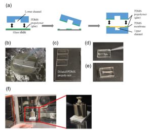
The PDMS sheet with the lower channel (lower sheet) is bonded to the PDMS membrane by using a PDMS prepolymer diluted with hexane (a dilution ratio of 1:3) as a glue1 (Fig.3a). Spin coat the diluted PDMS prepolymer (600 µL) at 2,000 rpm for 30 s on the surface of a glass slide (52 × 76 mm) to cover the slide with a thin layer of the glue and incubate it for 10 min to dry the solvent (Fig.3b). Place the lower sheet on the coated glass slide (Fig.3c). Apply glue at the four corners of the PDMS membrane bonded with the upper sheet (Fig.3d). Peel off the lower sheet from the glass slide and place the glue-coated surface of the sheet on the PDMS membrane (Fig.3e). After 30 min of incubation, bond the lower sheet to a cover slip by plasma bonding. Place a 1-kg weight and a glass slide on the device and bake it at 100˚C for 1 h (Fig.3f).

Fig.3 (a) Schematic diagram of bonding of the PDMS membrane and lower sheet. (b) Spin coat the diluted PDMS prepolymer (glue). (c) Lower sheet is placed on the thin film of the diluted PDMS prepolymer. (d) The diluted PDMS prepolymer is applied on the four corners of the PDMS membrane. (e)The glue-coated surface of the lower sheet is placed on the PDMS membrane. (f) A weight and a glass slide are placed on the device to bake it at 100˚C.

  1. Tubing

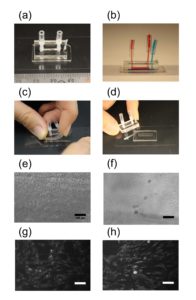
Connect polytetrafluoroethylene (PTFE) tubes (1 × 2 × 100 mm) with Tygon tubes (1.59 × 3.18 × 10 mm) to the holes present at both ends of the upper microchannel. Connect a PTFE tube (46 × 0.92 × 150 mm) to the hole of the lower channel. Apply PDMS prepolymer at the root of the tubes, and then bake it at 100˚C for 1 h for firm connection (Fig.4a and b).

  1. Cell culture

Introduce a cell suspension into the upper microchannel, which is manually precoated with 0.1 mg/mL of fibronectin. Incubate the device at 37˚C with 5% CO2 for 16 h to allow cells to adhere to the bottom of the upper channel (surface of the PDMS membrane).

  1. Detachment of the lower sheet for cell observation

Remove the lower sheet from the device carefully (Fig.4c and d). Place the rest of the device on a cover slip for observation with an inverted microscope (Fig.4 f and h).

Fig.4 (a) The complete microdevice. (b) Side view of the microdevice. The cell culture channel (upper) is filled with water containing a red food color, while the lower channel is filled with water containing a blue food color. (c) and (d) The lower sheet is peeled off from the microdevice carefully. Phase contrast images of cells (e) before and (f) after detachment of the lower sheet. Fluorescent images of cells stained with CellTracker Red CMTPX (g) before and (h) after detachment.

Conclusion

We developed a microfluidic device with a detachable lower microchannel. It is important that different bonding techniques be used for each side of the PDMS membrane. If the lower channel is filled with air and the device is incubated in a CO2 incubator, dew condensation is often observed in the lower channel when the device is taken out from the incubator. The condensation in the lower channel makes observation difficult (Fig.4e and g). This problem was solved with the detachable device.

Acknowledgment

This work was supported in part by the Japan Society for the Promotion of Science (JSPS) KAKENHI Grant Number JP16H04170.

Reference

  1. Chueh, B.H., Huh, D., Kyrtsos, C.R., Houssin, T., Futai, N., Takayama, S. (2007). Leakage-free bonding of porous membranes into layered microfluidic array systems. Analytical Chemistry 79 (9), 3504–3508.
Digg This
Reddit This
Stumble Now!
Share on Facebook
Bookmark this on Delicious
Share on LinkedIn
Bookmark this on Technorati
Post on Twitter
Google Buzz (aka. Google Reader)