Author Archive

Connector-less manipulation of small liquid volumes in microchannels

Christopher Moraes, Yu Sun, and Craig A. Simmons
Department of Mechanical and Industrial Engineering, University of Toronto, Toronto, Ontario, Canada

Why is this useful?


An often-touted advantage of microfluidic systems is the small volumes of reagents required.  However, the world-to-chip interconnects often require fluid volumes orders of magnitude greater than those used within the microfluidic channels themselves.  Moreover, commonly used interconnect schemes are either expensive; custom-manufactured or require substantial additional fabrication efforts; or are severely prone to failure, leaks and clogging.

This tip presents a simple, inexpensive and easily-accessible method to manipulate small volumes of fluid in standard microfabricated PDMS channels, without the use of a connector scheme.  Though it cannot be used to produce well-controlled or continuous long-term flow, we have found it ideal for applications such as device pre- and post-processing (e.g., chemical-based surface modification and immunostaining).  The technique is simple and robust, and has been used effectively both by experienced researchers and untrained, minimally supervised undergraduate students in a teaching lab.

What do I need?


  • Fully cured microfluidic PDMS device
  • Glass substrate
  • PDMS punch
  • 1 mL Pasteur pipette bulb (Sigma-Aldrich, product Z111589)
  • Pipettes and tips
  • Kimwipes

Figure 1

How do I do it?


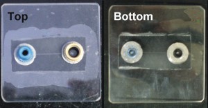
1. Punch an access port into the PDMS device at the channel entry and exit points.  The size of the hole can be selected based on the reagent volume required by the device.  In this example, we used a 1/8″ diameter punch.

2. Bond the patterned PDMS layer to a glass slide, as per standard procedure for PDMS device fabrication.

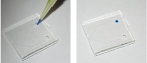
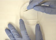
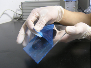
3. Pipette a small quantity of reagent directly into the access port (Figure 1; blue dye used for this demonstration).  We have successfully used this technique with volumes as low as 4 mu.gifL.

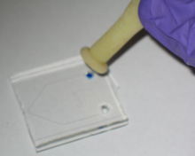
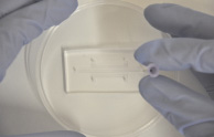
4. Place the Pasteur pipette bulb (Figure 2) over the punched reservoir and gently hold it down so it forms a conformal seal around the reservoir (Figure 3).  Provided the area around the access port is fairly flat, maintaining a seal is typically not a problem.

Figure 2

Figure 3

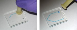
5. Squeeze the bulb gently to apply positive pressure and cause the fluid to flow into the microchannels (Figure 4).

Figure 4

6. Channels can be cleared by first pipetting away excess fluid from the access port, and then using the Pasteur pipette bulb to force air through the channel, while wicking away the expelled liquid at the exit port with a Kimwipe.

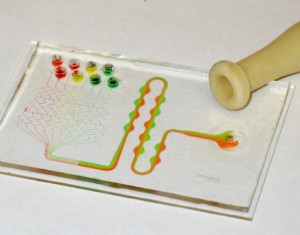
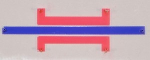
The Pasteur pipette bulb can also be used to apply a negative pressure by squeezing it first, placing it over the channel access port, and gently releasing the bulb.  In Figure 5, we used this technique to drive flow in a standard microfluidic gradient generator system:  negative pressure is applied at the outlet channel port, drawing eight separated reagents through the mixing channels.

Figure 5

Digg This
Reddit This
Stumble Now!
Share on Facebook
Bookmark this on Delicious
Share on LinkedIn
Bookmark this on Technorati
Post on Twitter
Google Buzz (aka. Google Reader)

Simple fabrication of microfluidic devices by replicating Scotch-tape masters

Anil B. Shrirao1 and Raquel Perez-Castillejos1,2
1 Department of Electrical and Computer Engineering, 2 Department of Biomedical Engineering, New Jersey Institute of Technology, Newark NJ, USA

Why is this useful?


We present a method for fabricating PDMS microfluidic devices based on replicating a master made of Scotch tape.  Often the fabrication of microfluidic devices by soft lithography is restricted to those who have access to a cleanroom that allows the fabrication of a master with micrometric features.  Here we demonstrate that patterned Scotch tape can be used (without the need of any chemical treatment) as a master for soft lithography yielding microfluidic devices with a uniform height of ~ 60 µm.  As a difference to previous Chips & Tips on rapid and easy prototyping techniques [1, 2], in this method the Scotch tape does not remain as part of the microfluidic device after fabrication.  Here we used a handheld cutting tool (scalpel) to pattern the Scotch tape.  A laser cutting machine could be used, instead, for masters requiring higher precision.

What do I need?


  • Glass slides, pre-cleaned from Manufacturer (Fisher Scientific, 75mm x 50mm x 1mm, Cat. No. 12-550-C)
  • Scotch tape (3M Scotch® Transparent Tape 600[6])
  • Stainless steel Scalpel or surgical blade with (Feather Safety Razor Co., LTD, Cat. No. 2976#11)
  • Polystyrene Petri dish (Fisher Scientific, 100mm x 15mm, Cat. No. 08-757-12)
  • Tweezers
  • Oven or hot plate (to work at 65°C)
  • Gloves (do not use latex gloves)
  • PDMS silicone elastomer base and curing agent (Sylgard 184, Dow Corning)

What do I do?


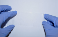
1. Attach a strip of Scotch tape to the glass slide.  The thickness of the Scotch tape will determine the height of the microchannel.  (To increase the height of the channel, attach additional strips of Scotch tape.)
2. Print the layout of the microchannel on regular paper.  Place the printout on a flat surface.
3. Place the glass slide on the printout, with the Scotch tape facing up.  Align the glass slide to the microchannel layout.  Fix the glass slide to the printout with a piece of Scotch tape on the corner of the slide.
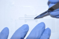
4. Use the scalpel to cut the tape on the glass slide according to the layout.  (For cutting, we used another glass slide as a ruler)
5. Remove the Scotch tape from all regions of the glass slide except those in the layout of the microchannel.
6. Place the glass slide with patterned Scotch tape in a heating oven at 65°C for 2-3min; this improves the adhesion of the edges of patterned Scotch tape to the glass substrate.  At this point, the Scotch-tape pattern does not need any further treatment in order to be used as a master for soft lithography [1].
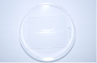
7. Mix the base and curing components of PDMS as recommended by the manufacturer [2].  Place the glass slide in a Petri dish, with the patterned Scotch tape facing up.  Pour the PDMS mixture in the Petri dish until the master (i.e., glass slide and Scotch tape) is covered completely.  Degas PDMS in vacuum (if needed) and allow it to cure for 1 hour at 65°C.
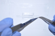
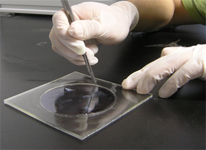
8. Use the scalpel to cut the slab of PDMS containing the microchannel.  Peel off the PDMS replica.  (The Scotch-tape master can be used again by repeating step 7.)
9. Punch holes in the PDMS replica for the inlets and outlets of the microfluidic device.
10. Seal the PDMS replica to a substrate, either (i) conformally-by bringing the PDMS replica in contact with a smooth, clean substrate-or (ii) irreversibly-by bringing the PDMS replica in contact with the substrate after oxidizing both parts in an oxygen plasma [3]).


Acknowledgements


R. P.-C. acknowledges the support of the New Jersey institute of Technology through starting faculty funds.

References


[1] R. J. Holmes and N. J, Goddard, Rapid prototyping of microfluidics, Chips & Tips (Lab on a Chip), 15 February 2007.
[2] R, Kumar, R. L. Smith, and M. G. Pappas, A method for rapid fabrication of microfluidic devices, Chips & Tips (Lab on a Chip), 30 June 2009.
[3] Y. Xia and G. M. Whitesides, Annu. Rev. Sci., 1998, 28, 153-184.
[4] Dow Corning Product Information, “Information about Dow Corning® brand Silicone Encapsulants”.
[5] M. K. Chaudhury and G. M. Whitesides, Langmuir, 1991, 7, 1013-1025.
[6] Scotch tape

Digg This
Reddit This
Stumble Now!
Share on Facebook
Bookmark this on Delicious
Share on LinkedIn
Bookmark this on Technorati
Post on Twitter
Google Buzz (aka. Google Reader)

Simple, low-cost, low-temperature cured adhesive rings for microfluidic ports

Johnny J. Perez and Jonathan G. Shackman
Department of Chemistry, Temple University, Philadelphia, PA, USA 19122

Why is this useful?


A critical step in fabrication of microfluidic devices is coupling with the macroscopic world.  Reservoirs or pressure fittings are frequently adhered to devices by liquid epoxies or heat cured adhesive rings, such as supplied with commercial Upchurch Scientific (Oak Harbor, WA, USA) NanoPorts.  Liquid methods can potentially enter the device and clog channels.  Non-tacky resin rings make alignment of critical fittings and O-rings difficult, as they are inert until heat cured.  As an alternative to PDMS-based interfacing [1,2,], we describe a simplified method for forming customized, tacky adhesive rings using 3MT VHBT pressure-sensitive tape (Fig 1).  The rings are similar to the now discontinued NanoPort rings formed from 3MT 583 tape [3], but can cure at room temperature.  We have tested NanoPorts using these rings underwater on both polycarbonate and glass substrates in excess of 40 psi with no failures.  The cost per ring (assuming a 1 cm diameter) is a few US pennies.  Rings can easily be peeled from the ports and substrate after applying sufficient torque or sheer forces without leaving residues, facilitating aggressive cleaning (such as in piranha solution) of clogged microchannels.

Figure 1

What do I need?


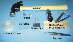
The materials needed are shown in Figure 2 and include:

  • 3MT VHBT tape.  We use 0.5″ wide VHBT 4926, but a variety of tapes (including 3MT 583 tape) could be used, with selectable adhesion qualities and solvent resistances.
  • Gasket Punch or Cork Borers.  Cork borers (commonly used in chemistry labs) require two cuts while dual cutting punches, such as available from McMaster-Carr (Elmhurst, IL, USA), cut both inner and outer rings simultaneously.  We use 3/16″ inner and 7/16″ outer diameter punches for NanoPort rings.
  • Hammer and pad.  A piece of scrap wood can be used for a cutting pad.
  • Forceps.  Fine tips aid in ring manipulation and removing the adhesive backing.
  • Ports and microchip.  Homemade or commercial ports and chips can be used with the method.  The glass device used for demonstration was made using previous protocols [4].
  • Binder clip.  The tape requires at least 10 psi for strong bonds and pressure should be maintained during curing.  Mini-vises or C-clamps can also be used for hard to reach ports [3].
  • Oven (optional).  VHBT tape can cure overnight at room temperature or in 1 hr at 60 to 90 °C.

Figure 2

What do I do?


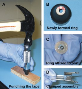
The sequence is shown in Figure 3.  The following specifics can easily be modified for a given application.

Figure 3

1. Clean ports / O-rings in DI water followed by methanol or isopropanol.  It is assumed the microdevice is clean after fabrication but can also be carefully cleaned.
2. Cut a 1 cm length of tape and place the sticky side on the punch.
3. Place the end of the punch/tape on a pad or wood block and hit the opposite end of the punch with a hammer (Fig 3A).
4. The ring will likely remain in the punch, with the backing side facing out (Fig 3B).  Use forceps to remove the newly formed ring and attach the exposed tacky side to the port.  Pressing the port (prior to removing the backing) against a flat surface can help adhesion.
5. Remove the backing with forceps to expose the other tacky side (Fig 3C) and align the assembly with the microchip access hole.
6. Clamp the port and microfluidic device using a binder clip or clamps (Fig 3D).
7. Cure either overnight or for 1 hr in an oven at 60 to 90 °C.
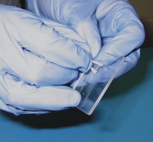
8. Adhered ports can be removed by either twisting and tilting or tightening a nut longer than the port to lift the port off the substrate.  The remaining ring can be removed using forceps to lift an edge and peeling (Fig 4).

Figure 4

What else should I know?


Rings should be made as needed to prolong shelf life (VHBT on the roll lists a 2 yr life when stored at room temperature and 50% relative humidity) [5].  While suitable for aqueous solutions, prolonged use of organic solvents is not recommended with VHBT tape [6], and an alternative adhesive or method, such as described by Watson and Wheeler [1], is suggested.  Application of high torque will cause the rings to fail, as can occur when over-tightening pressure fittings.

References


[1] M. W. L. Watson, A. R. Wheeler, Organic solvent compatible reservoirs for glass microfluidic chips, Chips & Tips, (Lab on a Chip), 12 December 2007
[2] J. Greener, W. Li, D. Voicu, E. Kumacheva, Reusable, robust NanoPort connections to PDMS chips, Chips & Tips, (Lab on a Chip), 24 October 2008
[3] C. Koch, J. Ingle, V. Remcho, Bonding Upchurch® NanoPorts to PDMS, Chips & Tips, (Lab on a Chip), 15 February 2008
[4] N.I. Davis, M. Mamunooru, C.A. Vyas, J.G. Shackman, Anal. Chem., 2009, 81, 5452-5459.
[5] 3MT VHBT Double Coated Acrylic Foam Tapes – June 2009 Data Sheet
[6] 3MT VHBT Durability – March 2001 Bulletin

Digg This
Reddit This
Stumble Now!
Share on Facebook
Bookmark this on Delicious
Share on LinkedIn
Bookmark this on Technorati
Post on Twitter
Google Buzz (aka. Google Reader)

Fast-iteration prototyping and bonding of complex plastic microfluidic devices

Jonathan Siegrist, Mary Amasia, and Marc Madou
Departments of Biomedical, Chemical, and Mechanical Engineering, University of California, Irvine, CA, 92697, USA

Why is this useful?


The fabrication and bonding of rapid-prototyped polymer-based microfluidic devices is of great interest. The emphasis is not only on the ability to produce large numbers of devices rapidly, but to perform fast design and test iterations. Here, we present a method for rapidly cutting thin plastic films into complex shapes, such that sophisticated 2.5-D microfluidic chips can be created. The plastic layers are bonded together using traditional, low-pressure thermal bonding to minimize channel deformation while achieving high bond strengths capable of withstanding high-pressure & temperature operations, such as polymerase chain reaction (PCR). The authors have found this method to be particularly amenable to fast design iterations, as one can easily go from a design on the computer screen to testing of a real part within 3 hours.

The method presented here of cutting plastic films using a commercially-available knife-based cutter/plotter avoids the use of traditional CNC milling, which can leave behind burrs and rough edges. While hot-embossing and laser machining can be superior alternatives to CNC milling, they are considerably more complex and expensive than the method presented here. Also, by using a computer-controlled cutter, obvious advantages are gained in terms of possible design complexity and reproducibility as compared to previous Tips [1, 2]. Finally, this cutting method can be used for many types of plastic films (< 400 um thick, depending on the machine being used) without the need for extensive optimization of cutting speeds or feed rates.

The use of thermal bonding allows for much higher bond strengths as compared to the use of pressure-sensitive adhesives or double-sided tapes, and also provides a large dynamic range in terms of the types of plastics that can be used. For example, thin films of either high glass-transition temperature (Tg) materials such as polycarbonate or low-Tg cyclic olefin copolymers can be used with this method, as compared to lamination methods that are limited to low Tg materials only [3].

What do I need?


  • Hydraulic Thermal Press, ideally with a max. temperature of at least 200ºC and a max. pressure of at least 1 MPa (the device used here was an MTP-8 from Tetrahedron Associates, Inc., CA, USA)
  • Computer-Controlled Cutter/Plotter (the device used here was a CE-2000 from Graphtec America, Inc., CA, USA)
  • CAD software
  • Bare Si Wafers, at least single-side polish
  • Plastic Films (the films used here were polycarbonate from McMaster-Carr, CA, USA)
  • Double-sided Tape (3M Scotch brand was used here)
  • Aluminium Foil
  • Tweezers
  • Alignment Pins (optional)
  • Oxygen Plasma System (optional)

What do I do?


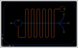
1. Design your microfluidic device using common CAD software (Fig. 1). Ensure the drawing for each layer is in a “polyline” format (i.e., each continuous line is defined as a single object) to facilitate smooth cutting. Import the CAD file into the software that controls the cutter/plotter.

A proof-of-concept microfluidic device laid out using CAD software, with different layers defined for each plastic part to be used.

2. Attach your plastic film (using double-sided tape) to a plastic sheet that will act as your support/sacrificial layer (e.g., 0.75 mm thick). Place this structure in the cutter/plotter, and cut the film (Fig. 2). Cutting force and number of cuts may need to be optimized depending on the film thickness. We found that 2x low-force cuts worked well for 127 µm-thick polycarbonate films, and 4x medium-force cuts worked well for 254 µm-thick films.

The plastic film to be cut is mounted on a support base using double-sided tape, and then placed in the cutter/plotter.

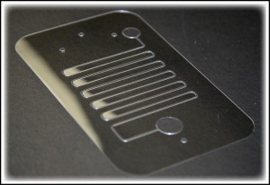
3. After all cuts are complete, carefully remove the part from the sacrificial layer and use tweezers to remove and discard the cut-out plastic features (Fig. 3). Repeat this for all layers, and then clean the plastic layers using isopropanol and water.

A single layer of polycarbonate cut out using the cutter/plotter, after removal of the cut features (for reference, the small loading and venting holes are 1 mm diameter).

4. Align all of the layers, and hold together using a clip. You may include alignment pin features on your layers, and use pins to assist in alignment. For example, you could use 1 mm-diameter pins (McMaster-Carr, CA, USA – #91585A001).
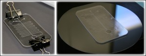
5. Place the assembled microfluidic device layers on the mirror-finished side of a Si wafer, and remove the clip(s) (Fig. 4). Then place the second wafer mirror-finished side down on top of the microfluidic device, being careful not to disturb the alignment.

All layers of the microfluidic device are aligned and held together using clips (left) and the part is then carefully placed on a Si wafer in preparation for thermal bonding (right).

6.  Place the assembly in the thermal press sandwiched between two pieces of foil, and thermally bond. Approximate parameters we found to work well for our proof-of-concept, multi-layer, polycarbonate device (1-top layer with loading/venting holes: 254 µm thick, 2-film with serpentine channel: 127 µm thick, 3-film with access holes and reservoirs: 127 µm thick, 4-film with linear channel: 127 µm thick, and 5-bottom layer: 254 µm thick) are shown in Fig. 5.

The thermal bonding parameters used for the proof-of-concept microfluidic device.

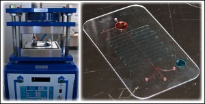
7.  Remove the microfluidic device from the thermal press, and test (Fig. 6).

The thermal press used (left) and the completed microfluidic device (right) loaded with contrast agents for visualization.

What else should I know?


Thermal bonding parameters, such as bonding temperature, pressure, dwell times, and ramping rates, will need to be optimized to ensure complete bonding of the plastic layers. The main disadvantage of thermal bonding is possible microchannel deformation, which can affect fluidic function. Thus, the Tg of your material, the number of layers, and the required bond strength will all need to be considered. The previous Tip on prevention of chamber-sagging has obvious uses here [4].

The limitations on feature size using this method should also be noted. The thickness (z-axis) of your channels/chambers is determined by the thickness of the films. We found the feature size (x-y plane) limitations when cutting films to be ~ 200 µm, as limited by the cutter/plotter being used. Newer machines list resolutions on the order of 10s of µm.

Finally, while these plastic parts are inherently hydrophobic, they can be made hydrophilic via oxygen-plasma treatment. Common plasma-treatment parameters for our devices are 200 W for 2 mins at 200 mTorr O2-pressure to provide hydrophilicity for many weeks. This can facilitate liquid loading and also serve as a sterilization step.

Acknowledgements


We would like to thank the DARPA-MF3 center for funding, and Dr. Albert Yee of UC Irvine for generously allowing us to use his thermal press.

References


[1] R. J. Holmes and N. J, Goddard, Rapid prototyping of microfluidics, Chips & Tips, (Lab on a Chip), 15 February 2007.
[2] R, Kumar, R. L. Smith, and M. G. Pappas, A method for rapid fabrication of microfluidic devices, Chips & Tips, (Lab on a Chip), 30 June 2009.
[3] D. Olivero and Z. Fan, Lamination of plastic microfluidic devices, Chips & Tips, (Lab on a Chip), 30 July 2008.
[4] J. Xu and D. Attinger, How to prevent sagging during the bonding or lamination of chips with large aspect ratio chambers, Chips & Tips, (Lab on a Chip), 24 July 2009.

Digg This
Reddit This
Stumble Now!
Share on Facebook
Bookmark this on Delicious
Share on LinkedIn
Bookmark this on Technorati
Post on Twitter
Google Buzz (aka. Google Reader)

Rapid prototyping of branched microfluidics in PDMS using capillaries

S. Ghorbanian, M. A. Qasaimeh and D. Juncker
Biomedical Engineering Department, McGill University and Genome Quebec Innovation Centre, McGill University, 740 Dr. Penfield Avenue, Montreal, QC, H3A 1A4 Canada

Why is this useful?


Polydimethylsiloxane (PDMS) is widely used for the fabrication of microfluidic systems because it can readily be molded into the desired shape, is easy to seal onto substrates, and is transparent thus permitting visualization of the sample [1]. However, the fabrication of PDMS microfluidic devices depends on a microfabricated mould that needs to be made in a clean room using photolithography and microfabrication methods, all of which are costly and time consuming and beyond the reach of many researchers. Rapid prototyping techniques that circumvent the requirement for a clean room have been proposed, such as the use of double sided scotch tapes, but lack precision and control [2,3].

Here we present a method for rapid prototyping of branched microfluidics in PDMS with control over the architecture, channel width and depth. We propose using capillaries as the mould.  They are cut to size, then arranged on a flat PDMS according to the desired architecture and covered with PDMS which is then cured. The size of each channel can be adjusted by selecting a capillary with the desired diameter, and different branch architectures can readily be produced. The capillaries are then simply removed from the PDMS replica and leave behind a network of channels.

A key challenge is the gaps formed at the intersections between abutting capillaries. We found that a small flake of paraffin can be used which is then melted to fill up this gap. The use of capillaries with a square cross-section further facilitates the moulding, and allows for making complex networks with ease and good yield. This protocol only requires materials which are commercially available and comparatively inexpensive and takes less than one hour of hands-on time, followed by three hours of curing.

What do I need?


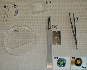
1. A layer of flat cured PDMS, Figure 1d
2. Uncured PDMS
3. Petri dishes
4. Square capillaries (preferably) or circular capillaries [4], Figure 1a
5. Ceramic cutting stone [4], Figure 1b
6. Paraffin [5], Figure 1c
7. Oven or hot plate
8. Sharp tweezers and razor blade, Figure 1(e,f)
9. Double-sided tape [6]

Figure 1. Required materials: (a) Glass capillaries, (a1) Cross section of the square glass capillary and (a2) the round glass capillary [4]. (b) Capillary cutting stone [4]. (c) Paraffin flakes [5]. (d) Flat cured PDMS piece in a Petri dish. (e) Razor blade. (f) Tweezers


What do I do?


1. Cure a layer of PDMS in a Petri dish. Remove the PDMS, and cut it to the desired size. Flip this piece to obtain the flat surface on top and place it inside another Petri dish as shown in Figure 2.
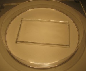
Figure 2. Flat piece of a cured PDMS

2. Cut two pieces of capillary, Figure 1a (or as many needed to make the branched channels) using a ceramic cutting stone. The capillaries should be cut to a length that facilitates handling, typically three or more times the length of the final channels of interest and shorter than the diameter of the Petri dish. Also see “What else should I know I”. After cutting the capillaries, dip their tip at each side in melted paraffin or liquid glue and let it solidify. This helps prevent air trapped in the capillaries from exiting while degassing the PDMS, which can lead to bubbles and displacement of the capillaries.

3. Under the stereomicroscope grind the tip of the capillaries (which will be making the connections between capillaries) to remove the bumps seen in Figure 3a using a polishing stone, such as the side surface of a cutting stone, with horizontal movements, Figure 3b and flatten the tip completely, Figure 3c, which can be done at angles other than 90 degress as well, Figure 3d.

Figure 3. A square capillary before (a) and after grinding with the ceramic stone (b) and flattening its tip into a right angle (c) and other angles (d)

4. Stick double-sided tape at the outer extremities (preferably not at the connection sites) where the capillaries will be placed on the flat PDMS in the Petri dish, Figure 4a. Under a stereomicroscope place the capillaries according to the desired architecture. Figure 4b illustrates the placement of capillaries for fabricating T-shaped microchannels.
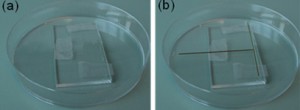
Figure 4. Placing the capillaries on the flat PDMS held by double side tape

5. Examine the gaps and connections between the capillaries to ensure good contact. A T-shaped connection and 45 degree connections are shown in Figure 5 below.
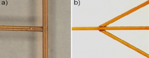
Figure 5. Different connections between capillaries: (a) Capillary connection in T-shape with a right angle and (b) connections with acute angles

6. Carefully place a small piece of paraffin using sharp tweezers on each of the capillary connections, Figure 6a. Heat the tip of the tweezers on a hot plate for a minute, and then carefully approach the tip to melt the paraffin, which fills the gaps between the capillaries due to capillary effects and joins them to one another, Figure 6b. The excess melted paraffin can be removed carefully wiht the tip of a razor or sharp tweezers.
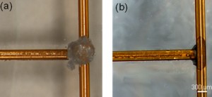
Figure 6. Filling the interconnection gaps with melted paraffin. (a) Piece of paraffin placed on the connection site. (b) The connection site with melted paraffin after cleaning

7. Pour a layer of uncured PDMS over the connected capillaries as shown in Figure 7 and degas the PDMS by placing the Petri dish in a vacuum desiccator to remove all air bubbles, for alternative methods see “What else should I know II”. Then, place the Petri dish in the oven at 65°C for 3 hours or more. For shorter curing time see “What else should I know III”.
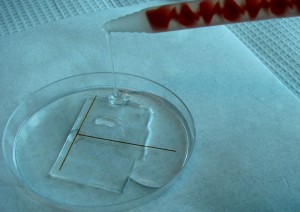
Figure 7. Pouring uncured PDMS over the capillaries network

8. Remove the whole piece of cured PDMS from the Petri dish. Cut the sides of the cured PDMS using a razor blade, leaving a significant amount of the capillary exposed outside as shown below. Then carefully pull out the capillaries from the sides of the PDMS using pliers as shown in Figure 8. To make this process easier, the network can be immersed into or washed with acetone which will swell the PDMS and expand the channels prior to pulling out the capillaries.
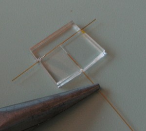
Figure 8. Pulling off the capillaries after the PDMS is fully cured

If residues of paraffin are left inside the microchannels these can be dissolved and washed by flushing the microchannels with acetone.

9. Trim the microfluidic device to the desired shape using a razor blade or a cutter, Figure 9.
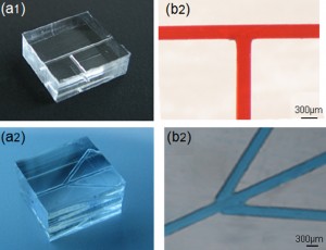
Figure 9. Fabricated branched microfluidics (a). Microchannels filled with red and blue dye (b).

What else should I know?


Several alternative fabrication tips are listed below:

I) To fabricate an open channel microfluidic network replace the flat cured PDMS layer (in step 1) with a clean glass slide. Once the PDMS is cured it can be separated from the glass slide. In this process smaller capillaries can be used to make the channels which can be removed using tweezers after detaching the PDMS from the substrate. This open network can also be bonded to another PDMS layer after the capillaries are removed.
II) If no vacuum desiccator is available to degas PDMS, the sample can be left to be degassed and cured at room temperature overnight followed by post-curing in an oven at 65°.
III) To increase the speed of PDMS curing in step 8, the Petri dish may be replaced by an aluminum foil or a glass plate and allow to use much higher temperatures inside an oven or on a hot plate to cure the PDMS within a few minutes.
IV) It is preferable to use square capillaries because there are no gaps formed at the connection sites due to the square shapes of the capillaries as opposed to the round capillaries which will have a small gap formed at the connection sites due to the rounded shape of the capillary walls, Figure 1(a1). These gaps can, however, get filled with melted paraffin.

References


[1] D. Duffy, J. McDonald, O. Schueller, G. Whitesides, Rapid prototyping of microfluidic systems in poly (dimethylsiloxane), Anal. Chem., 1998, 70, 4974-4984.
[2] R. J. Holmes and N. J, Goddard, Rapid prototyping of microfluidics, Chips & Tips, (Lab on a Chip), 15 February 2007.
[3] R, Kumar, R. L. Smith, and M. G. Pappas, A method for rapid fabrication of microfluidic devices, Chips & Tips, (Lab on a Chip), 30 June 2009.
[4] Polymicro technologies
[5] Fisher Scientific
[6] Scotch Tape

Digg This
Reddit This
Stumble Now!
Share on Facebook
Bookmark this on Delicious
Share on LinkedIn
Bookmark this on Technorati
Post on Twitter
Google Buzz (aka. Google Reader)

Reversible high contact bonding of microscope slide chips

Jian Hua Han, Shao Hua Li, Zhong Han Sheng and Long Jiang
Key Laboratory of Colloid and Interface, Institute of Chemistry, Chinese Academy of Sciences (ICCAS), Beijing, China

Why is this useful?


We demonstrate a reversible bonding method to fabricate microscope slide glass chips. This method involves pre-curing a PDMS polymer layer to form a highly adhesive glue which strongly bonds glass chips. Traditional bonding methods[1-4] are either irreversible or not very strong; our approach solves this problem. The glass chips made by our approach can bear high fluid pressure without leakage and can easily be disassembled and reassembled when clogging happens. Our method is suitable for any ordinary labs that lack expensive equipment to fabricate microfluidic chips.

What do I need?


  • Microscope slides and PDMS kits (SYLGARD®184), produced by Dow Corning. The silicone elastomer base and curing agent were mixed well at the ratio of 10:1 to form a paste before use.
  • Craft knife, scalpel, plastic wrap, etc.
  • Microscope slides chip with patterns and appropriately located inlet and outlet holes.

What do I do?


First, prepare a microscope slide chip using standard wet etching methods[5] and drill holes. Then execute the following 5 steps:

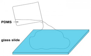
1. Pour the PDMS (elastomer mixed with curing agent and degassed) onto a glass slide, see figure 1.

Figure 1

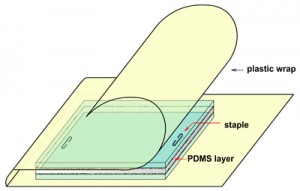
2. Place another glass slide onto the PDMS of step 1 carefully, avoiding any bubbles during the process. Use a staple as a spacer, and wrap the sandwich in plastic wrap to avoid leakage of PDMS. See figure 2.

Figure 2

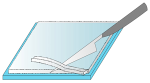
3. Cure the PDMS to a solid state, then pry up the upper slide. Use a scalpel to trim the PDMS layer to size, see figure 3.

Figure 3

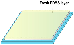
4. Spin coat a fresh PDMS layer 1µm thick onto the PDMS layer of step 3 at the rate of 3000 RPM, then pre-cure for 20min at 80°C to form a hard glue, see figure 4.

Figure 4

5. Place the glass slide chip (with patterns and appropriately located inlet and outlet holes) onto the PDMS layer of step 4, then continue to cure the polymer to a solid state, and the microfluidic chip is formed, see figure 5.

Figure 5

What else should I know?


The method presented above is a useful method for rapid fabrication of microfluidic chips. The advantages of this method are as follows:

  • does not need a strictly flat surface, very cheap microscope slides are available
  • high contact bonding strength, does not rupture under high pressure (280kPa), while commonly used devices cannot withstand fluid pressures of more than 100kPa
  • the chip can be opened with a craft knife when clogging happens and can be reused many times

The limitation of this method is that you must be careful when placing the etched glass slide onto the uncured PDMS layer – avoid too much pressure on it since this could lead to squeezing of PDMS into the channels and clogging of the chip.

Acknowledgements


This research is funded by the Chinese Academy of Sciences (grant number KJCX2-YW-H18) and the National Sci-Tech Special Item for Water Pollution Control and Management (2009ZX07 5287- 007 – 03).

References


[1] N. Miki, Sensor Letters, 2005, 3, 263-273
[2] A. Sayah, D. Solignac, T. Cueni and M. A. M. Gijs, Sensors and Actuators A: Physical, 2000, 84, 103-108
[3] S. Shoji, H. Kikuchi and H. Torigoe, Sensors and Actuators A: Physical, 1998, 64, 95-100
[4] N. Chiem, L. Lockyear-Shultz, P. Andersson, C. Skinner and D. J. Harrison, Sensors and Actuators B: Chemical, 2000, 63, 147-152
[5] M. Castano-Alvarez, D. F. Pozo Ayuso, M. Garcia Granda, M. T. Fernandez-Abedul, J. Rodriguez Garcia and A. Costa-Garcia, Sensors and Actuators B: Chemical, 2008, 130, 436-448

Digg This
Reddit This
Stumble Now!
Share on Facebook
Bookmark this on Delicious
Share on LinkedIn
Bookmark this on Technorati
Post on Twitter
Google Buzz (aka. Google Reader)

Easy and reversible connection with patafix for a pressure flow control system

Ayako Yamada, Fanny Barbaud, Yong Chen, and Damien Baigl
Department of Chemistry, Ecole Normale Superieure, Paris, France

Why is this useful?


Controlling flows in a microfluidic channel by gas pressure is sometimes preferable due to the stability and quick response of flows. Here we describe an easy way of connection between a sample reservoir and tubing connected to a pressure regulator without gas leakage. With our tips, one can quickly prepare a sample reservoir; one can easily open and close it to refill during experiments; one can easily disassemble, clean, and reuse the system, if necessary. It is also possible to manage a small volume sample (e.g., 5 µL) by employing a micropipette tip.

What do I need?


1. Patafix from UHU GmbH & Co. KG (Baden, Germany)
2. Plastic syringe without plunger (for a large volume sample; e.g., 100 – 1000 µL)
3. Needle for the syringe without pointed tip (for a large volume sample; e.g., 100 – 1000 µL)
4. Micropipette filter tip (for a small volume sample; e.g., 5 µL)
5. Tubing
6. Compressed air
7. Pressure regulator
8. PDMS channel


For a large volume sample (e.g., 100 – 1000 µL)


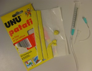
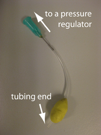
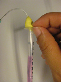
1. Wrap patafix around tubing to make a ball of approximately 1.5 cm diameter, leaving 5 mm from the tubing end (Fig. 1). The other end is to be connected with a pressure regulator. Put suitable accessories for your system.

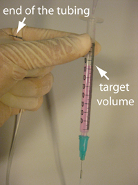
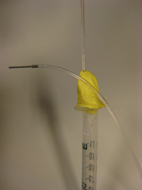
2. Connect a plastic syringe, a needle, and tubing. Hold the other end of the tubing, which is to be connected with your microfluidic channel, higher than the target volume in the syringe. Then fill the syringe with your sample using a micropipette (Fig. 2). Remove air bubbles by tapping, if necessary.

Figure 1

Figure 2

3. Insert the tubing with patafix prepared in step 1 to the open part of the syringe. Then squeeze the patafix into the syringe with your fingers so that about 5 mm of the syringe becomes filled (Fig. 3).

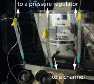
4. You can keep the tubing end accesible by sticking it on the patafix ball (Fig. 4). Connect the syring tubing to the pressure regulator keeping the syringe vertical. Following this way, your sample never touches patafix. It is convenient to place the pressure regulator high enough so that you can hang up the syringe from the regulator and maintain it vertical.

Figure 3

Figure 4

5. Connect the tubing with your channel and apply pressure (Fig. 5). This system can withstand operating pressures up to about 700 mbar (gauge pressure). You can open it by pulling the patafix out of the syringe, and easily refil with the sample, if necessary. If the tubing end is buried in patafix, simply tear off patafix until the tubing end appears. It is better not to try to dig patafix. It makes patafix go inside the tubing.

Figure 5

For a small volume sample (e.g., 5 µL)


1. Same as the step 1 described above, except that the diameter of the patafix ball should be about 2 cm.

2. Take your sample by micropipette. A pipette tip with a filter is preferable.

3. Remove the tip from the micropipette. If air comes up into the tip, you can get rid of it by tapping the tip gently until your sample goes back to the tip end. Then insert the tip into a PDMS channel inlet (we make inlet holes by punching through the PDMS with a syringe needle without a pointed tip and cleaning with isopropanol) (Fig. 6).

Figure 6

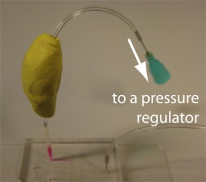
4. Connect the tubing and patafix prepared in the step 1 with the pipette tip. Try to make a homogeneous thickness (about 5 mm) layer of patafix around the connection and seal well (Fig. 7). Connect them to the pressure regulator and apply pressure. This system can withstand operating pressures up to about 300 mbar (gauge pressure).

Figure 7
Digg This
Reddit This
Stumble Now!
Share on Facebook
Bookmark this on Delicious
Share on LinkedIn
Bookmark this on Technorati
Post on Twitter
Google Buzz (aka. Google Reader)

A simple and economical holder for casting PDMS chips

Gang Li*, Qiang Chen and Jianlong Zhao

Shanghai Institute of Microsystem and Information Technology, Chinese academic of Sciences, Shanghai, China

Why is this useful?


To fabricate PDMS chips, one usually pours an un-cured PDMS mixture into a Petri dish or an aluminum foil tray containing the patterned master, and then cures for 2 h at 85°C. However, these casting dishes or trays present some cost problems. Often a relatively high consumption of PDMS is demanded for these casting holders because quite a part of PDMS will seep into the gap between the wafer and trays due to capillary forces during PDMS pouring. On the other hand, the seepage of PDMS under the master wafer may tilt the master causing the thickness of the PDMS mold to vary from one side to the other. Furthermore these casting dishes or trays are generally throw-away holders for casting PDMS chips, which also increases the fabrication cost of PDMS chips.

This tip presents a new casting holder, made of a hollow plate whose bottom is enveloped by an adhesive tape. This casting holder can simplify the operation of releasing the cured PDMS casting, and minimize the consumption of PDMS. In addition, this holder can be used to fabricate double-side flat PDMS chips by placing a flat substrate on its top.

What do I need?


  • Circular hollow plate (home-made of PMMA)
  • Adhesive tape (Nitto Denko Corp., SPV-224)
  • PDMS (Dow Corning Sylgard 184)
  • Hotplate (Chemat Technilogy Inc., KW-4AH hotplate)
  • PET (Polyethylene terephthalate) film and flat glass slide (for optional double-side flat PDMS chips)  

What do I do?


1. Seal the bottom opening of the hollow plate with adhesive tape to form a casting holder (Figure 1), whose diameter is a little bigger than that of master wafer.

Figure 1

2. Place the master in the holder, and carefully apply a pressure to attach it to the tape, preventing any gaps from forming at the interface (Figure 2).

Figure 2

3. Mix the PDMS according to the manufacturer’s procedure [1].

4. Pour the PDMS mixture in the casting holder, and then place the holder on a hotplate at 85ºC for 2 hours.

5. Once the PDMS is cured, remove the holder from the hotplate and allow it to cool to room temperature.

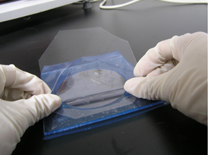
6. Gently peel off tape from the bottom of holder (Figure 3).

Figure 3

7. Carefully cut around the edge of the PDMS mold using a sharp scalpel, and separate the PDMS from the holder (Figure 4).

Figure 4

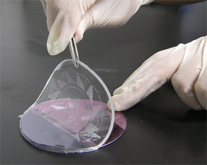
8. Finally, peel the PDMS mold from the master wafer (Figure 5).

Figure 5

9. (Optional, for double-side flat PDMS chips) Prepare the casting holder as described above,  pour the PDMS mixture in the casting holder until the level of PDMS is a little higher than the top of holder, and then carefully drop a PET film onto the prepolymer mixture (Figure 6), which provides an easy way to remove the cover plates from the PDMS molds after curing.

Figure 6

10. Apply a pressure on the top of the film with a stack of glass slides and steel block to planarize the surface of the PDMS chips, and then cure the PDMS by placing the holder on a hotplate (Figure 7).

Figure 7

11. After curing, remove the glass slide and steel block from the top of holder, and then gently peel off the tape and PET film from the PDMS block (Figure 8).

Figure 8

12. Finally, separate the PDMS block from the holder and peel the PDMS mold from the master.

Acknowledgements


This material is based upon work supported by the Major State Basic Research Development Program of China (No. 2005CB724305), and the National High Technology Research and Development Program of China (No.2006AA02Z136).

References


[1] Dow Corning Product Information, “Information about Dow Corning® brand Silicone Encapsulants,” 2005.

Digg This
Reddit This
Stumble Now!
Share on Facebook
Bookmark this on Delicious
Share on LinkedIn
Bookmark this on Technorati
Post on Twitter
Google Buzz (aka. Google Reader)

“Custom made” production of cheap Luer lock adapters for chip-to-syringe interfacing

Stefania Mazzitelli, Stefano Focaroli and Claudio Nastruzzi
Department of Chemistry and Technology of Drugs, University of Perugia, Perugia, Italy

Why is this useful?


One of the standard procedure to pump solutions, emulsions or suspensions, into microfluidic chips is based on the use of syringes, through peristaltic pumps. Syringe pumps are usually preferred over peristaltic ones, for their ease of use, for the accurate and stable control of the flow rate and, finally, for the possibility to employ sterile conditions.

Luer taper is a standardized system of small-scale fluid fittings used for making leak-free connections between a male-taper fitting and its mating female part on medical and laboratory instruments, including hypodermic syringe tips and needles or stopcocks and needles. The fitting is named after the 19th century German medical instrument maker Hermann Wülfing Luer.

There are two varieties of Luer Taper connections: Luer-Lok and Luer-Slip; Luer-Slip fittings simply conform to Luer taper dimensions and are pressed together and held by friction (they have no threads). Luer components are manufactured either from metal or plastic and are available from many companies worldwide but they are usually sold in few standard dimensions and are relatively expensive.

In this Tip we present a way to easily produce a variety of “on demand” Luer connectors, including: (a) female Luer x female Luer adapter, (b) female Luer x female Luer elbow, (c) male Luer x male Luer adapter, (d) male Luer x male Luer elbow, (e) male Luer x female Luer coupler and finally (f) male Luer x female Luer elbow.

What do I need?


  • 1-30 mL polypropylene syringes (Artsana, Italy) [1]
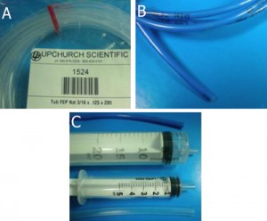
  • tubing: Upchurch Scientific® FEP (fluorinated ethylene-propylene); Tub FEP Nat 3/16 x .125 x 20ft (Upchurch Scientific, UK; No.: 1524) [2]
  • tubing: Timmer-Pneumatik GmbH; H-PTFE-4/2 mm (OD/ID)-blue, catalog Timmer 2001 [3]
  • Aesculap scalpel blades fig. 23, carbon steel, package of 100 pieces in dispenser package [4]
  • Aesculap scalpel handle fitting no. 4 for blades 18-36, 135 mm, 5 ¼, [5]
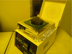
  • Black & Decker heat gun, model kx1693, [6]

What do I do?


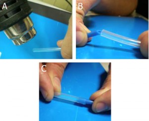
1. Tubing (A, B) and template syringes (C) are used for the production of Luer connectors. A: FEP (fluorinated ethylene-propylene) tubing; B: H-PTFE tubing.

Figure 1

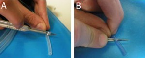
2. Tubing cutting by scalpel. The length of the Luer connector can be adjusted depending on the specific needs of the researcher (for instance, the distance between the syringe pump and the chip). Note that in the case of H-PTFE tube (B), the cutting is made with an angle of 45° with respect to the tube major axis.

Figure 2

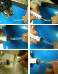
3. Preparation of a female Luer adapter: A. Heating of a FEP tube end by heat gun for 1-3 min; B-D. Press and insert the male Luer of a polypropylene syringe into the heated tube. E. Cool down the tube by tap water. F. Permanent deformation of the tube end.

Figure 3

4. Preparation of a male Luer adapter: A. Heating of a FEP tube end by heat gun for 1-3 min; B-C. Press and insert the H-PTFE tube end (cut at 45°) into the heated FEP tube, cool down the tube connection by tap water until a permanent deformation is reached.

Figure 4

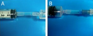
5. Examples of female Luer X female Luer adapter (A) and female Luer X male Luer adapter (B).

Figure 5

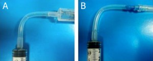
6. Examples of female Luer X female Luer elbow (A) and female Luer X male Luer elbow (B).

Figure 6

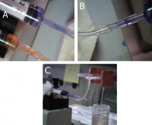
7. Examples of the use of female Luer X female Luer adapter to connect syringes to a commercial chip.

Figure 7

8. Examples of the use of female Luer X male Luer elbow to connect syringes to a homemade chip.

Figure 8

References


[1] http://www.artsana.com
[2] http://www.upchurch.com
[3] http://www.pneumatica-it.timmer-pneumatik.de
[4] http://www.chirurgische-instrumente.info/en/search.html?kw=bb523
[5] http://www.chirurgische-instrumente.info/en/search.html?kw=bb084r

Digg This
Reddit This
Stumble Now!
Share on Facebook
Bookmark this on Delicious
Share on LinkedIn
Bookmark this on Technorati
Post on Twitter
Google Buzz (aka. Google Reader)

A novel method for fabrication of reusable microfluidic interconnects

Koesdjojo, M.T., Mandrell, D.T., Tennico, Y.H., Remcho, V.T.*
Department of Chemistry, Oregon State University, Corvallis, Oregon, USA

Why is this useful?


The lack of an efficient interface, or interconnect, between microfluidic devices and the macroscale world is a major impediment to the broader application of micro total analysis system (µTAS). There are a number of current products and solutions available that seek to address this issue. An example of a simple approach is the direct integration of tubing or a syringe needle into the microchip inlet using epoxy glue.[1] However, direct connection to the inlet reservoir using an epoxy often leads to clogging of the microchannels. Commercially available connections to microfluidic chips and devices, such as the NanoPort from Upchurch Scientific (Oak Harbor, WA, 98277, USA), accommodate these needs by use of a threaded nut and ferrule system. These fittings can be integrated onto chip reservoirs by means of adhesive rings or epoxy glue.[2] The drawback to this method is that NanoPorts require the use of an epoxy glue that takes time to cure and is non-removable, or an adhesive ring that is not compatible with many solvents. Another drawback is that the epoxy requires high temperatures for complete curing, making it incompatible with low glass transition (Tg) polymers.[3] Commercial edge connectors provide efficient interfacing and allow rapid connections and reusability.[4] However, they are designed to be interfaced to a standard microchip format; which limits the compatibility of other chips with different geometries layout or sizes.

This tip presents an alternative approach to making simple, cost-effective universal interconnects. The device was developed to allow for standard compression tubing connectors, such as those available from Upchurch, to be interfaced with microfluidic chips. A standard breadboard fixture was used to compress the ports against the chip to apply sealing pressure, preventing leaks at the interface.  This method allowed for connections to be made without glue, epoxy, or any form of bonding, enabling the components to be easily and quickly reused or reconfigured without the need to machine new fixtures or re-bond ports. The working pressure of these ports was tested with a syringe pump, and withstood pressures in excess of 1000 psi without any signs of leakage or failure.

What do I need?


  • 0.25 and 0.5 inch thick plastic substrates such as polycarbonate (PC)
  • #21, #9 drill bits
  • 10-32 bottoming tap
  • 1mm drill bit
  • 1/16 inch PEEK or Teflon tubing
  • stainless steel 10-32 socket head cap screws
  • 1/32 inch Silicon o-rings
  • Upchurch 10-32 ferruled fittings (F-333)

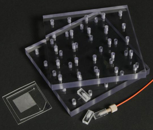
Figure 1. Picture of system components

What do I do?


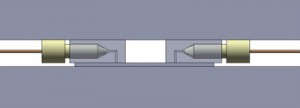
1. The first component was a port which allowed a standard ferruled connector to be attached perpendicular to the microfluidic device.  It contained a threaded portion for the fitting and a fluid path with small port on the bottom for the interface (Figure 2). The port was manufactured using 0.25 inch PC, but can be made of any material thick enough to allow room for the ferruled connector between the compression plates.  It was machined to size using a knee mill.  The threaded port was drilled with a #21 drill bit, then tapped with a 10-32 bottoming tap.  The fluid paths were drilled using a 1mm drill bit (substitute any drill to achieve the desired internal volume).  An o-ring was then placed in the threaded hole to ensure a tight seal against the ferruled fitting.

Figure 2. Interconnect section view (left) and the solid model (right).

2. The second component was a breadboard clamp which applied pressure between the microfluidic device and interconnects (Figure 3). This breadboard approach was particularly useful for prototyping devices having different dimensions and port locations, as interconnects could easily be relocated. A wide variety of bolt locations in the clamping plates allowed for a wide variety of component sizes and configurations. The breadboard clamp assembly was manufactured by cutting 0.5 inch thick PC into two five inch squares.  Using the knee mill, a one inch grid of holes was drilled and taped on one plate with the #21 drill and 10-32 tap.  Clearance holes were drilled on the same grid, using a #9 drill bit, in the second clamping plate.

Figure 3. Side view of a chip, interconnects, and the compression plates.

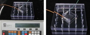
3. The 90° interconnect ports were placed on each of the reservoir holes of a microchip. The ferrules were connected to their respective tubing.  The top plate of the breadboard clamp was installed and using the holes closest to the sides of the chip, 10-32 stainless steel screws were inserted to apply even pressure by clamping the entire fixture.  Figure 4 shows the setup used to pressure-test the manufactured ports.

Figure 4. Setup used for pressure testing (left) and the close up view of a chip in the device (right).

References


[1] T. Das, Interfacing of microfluidic devices, Chips & Tips (Lab on a Chip), 27 February 2009.
[2] http://www.upchurch.com/
[3] J. Greener, W. Li, D. Voicu, E. Kumacheva,  Reusable, robust NanoPort connections to PDMS chips, Chips & Tips (Lab on a Chip), 8 October 2008.
[4] http://www.dolomite-microfluidics.com/

Digg This
Reddit This
Stumble Now!
Share on Facebook
Bookmark this on Delicious
Share on LinkedIn
Bookmark this on Technorati
Post on Twitter
Google Buzz (aka. Google Reader)