Author Archive

Periodic degassing of PDMS to create a perfect bubble-free sample

Jonathan C. Chen, Shengjie Zhai and Hui Zhao
Department of Mechanical Engineering, University of Nevada, Las Vegas NV, USA

Why is this useful?

The process of mixing the base and curing agent of PDMS often leads to air bubbles within the prepolymer due to its chemical reaction. The presence of air bubbles significantly decreases the strength and diaphaneity of the PDMS chip. Therefore, removing bubbles from PDMS becomes necessary and important.  The traditional degasing method is at least 2 hours for a 10g PDMS mixed solution, which appears too long. A way to shorten the degasing time is in need.

Here, we develop a simple and robust method to speed up the degasing process. By periodically stopping the pump and pulling out the hose, we can remove the bubbles by forcing them to burst since the bubble cannot withstand the dramatic change in pressure, considering the large difference between the low pressure inside the vacuum and the higher atmospheric pressure outside. Using this process, we can speed up the process by around 40 minutes (10-15 gram PDMS solution) and fabricate a smooth and bubble-free PDMS sample for any purpose, especially for optical applications. In practice, this time reduction may depend on the vacuum itself and the volume of PDMS solution.

What do I need?


  • SYLGARD 184 silicone elastomer base & curing agent (Dow Corning)
  • 1 Disposable polystyrene weighing dish (LxWxH 86mm x 86mm x 25mm, white)
  • Gast Doap 704aa compressor vacuum pump 18 HP 115 Vac
  • Bel-Art vacuum chamber and plate (Interior volume 0.21 cu. ft.)
  • IKA Ceramag Midi magnetic stirrer ceramic hot plate (50-1200RPM)
  • 1 magnetic stirring rod octahedral 1” x 5/16”

What do I do?


  1. Weigh the PDMS base and curing agent (10:1) in the weighing dish.
  2. Mix the base and curing agent together mechanically with a magnetic stirrer. (About 1000RPM to 1200 RPM)
  3. Move the dish to assure that the stir bar is around all sides of the weighing dish for proper mixture for about 10-20 minutes. (Depending on amount of PDMS used)
  4. Place the mixed sample into the vacuum chamber, turn on the pump, and leave for about 10 minutes.
  5. After the 10 minutes, there should be a significant amount of air bubbles appearing on the surface. Turn off the pump, quickly pull the vacuum chamber valve out, and let outside air in. Such action changes the pressure of the vacuum chamber, eliminates most of the big surface bubbles, and pulls out the small bubbles in the solution.
  6. Place the hose back on and turn on the pump again.
  7. Repeat step 5 and step 6 until there are no more bubbles on the surface and in the solution.
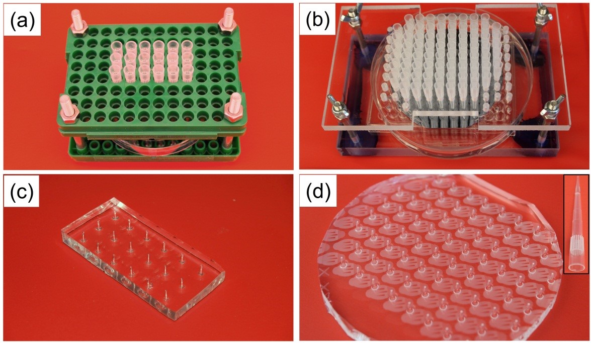
  8. Cast the treated PDMS over the desired mold, e.g. a patterned wafer.
  9. Cure at 65°C for 1.5 hours.

What else should I know?


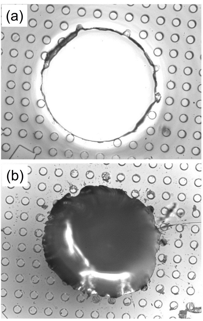
If the PDMS is used as a mold and placed in a petri dish with a microscopic glass slide, air bubbles will be significantly harder to remove due to bubbles trapped under the slide. This generally requires longer time within the vacuum and the occasional displacement of the slide to release any trapped air bubbles.

Another thing to note is that when casting the treated PDMS onto the desired mold; make sure not to pour out the mixture too fast. The slower the mixture is poured in, the less likely there will be air bubbles created during the transfer. If the sample generates air bubbles during the casting step, placing the product in the vacuum again for another 10 minutes will eliminate any unwanted bubbles.

Fig 1

Figure 1: Measure out a 10:1 ration of base to cure.

Fig 2

Figure 2: Mechanically stir the mixture.

Fig 3

Figure 3: Turn off the pump and use the difference in pressure to eliminate the bubbles.

Fig 4

Figure 4: Pour the mixture into the desired mold slowly.

Fig 5

Figure 5: Cure at 65°C for 1.5 hours.

Fig 6

Figure 6: The fabricated PDMS sample without bubbles.

Fig 7

Figure 7: The PDMS sample with a microscopic slide placed in.


Digg This
Reddit This
Stumble Now!
Share on Facebook
Bookmark this on Delicious
Share on LinkedIn
Bookmark this on Technorati
Post on Twitter
Google Buzz (aka. Google Reader)

Microchannels and chambers using one step fabrication technique

Vivek Kamat, KM Paknikar and Dhananjay Bodas*
Centre for Nanobioscience, Agharkar Research Institute, GG Agarkar road, Pune 411 004
E-mail: dsbodas[at]aripune.org; Tel: +91-20-25653680      

Why is this useful?       


At present many techniques are employed for fabricating channels and chambers, most of them using photolithography and soft lithography [1]. The fabrication of a circular channel and chamber in a monolithic design is challenging, which can be achieved using copper wires of varying diameters (from 20 µm). This simplistic process also eliminates usage of expensive equipment, can be performed in a normal laboratory environment (doesn’t require clean room facilities) and high fidelity structures could be obtained.      

Fabrication of chambers can be achieved in a simple, fast and novel approach by utilizing agarose gel. Agarose gel is an important component used in molecular biology experiments. Agarose powder is mixed with water and is boiled, after cooling the liquid polymerizes to form a gel. This gel can be utilized to mold the desired chamber (variable size and shape) which can be utilized for making chambers on chip.      

What do I need?      


  1. PDMS (1 part curing agent and 10 part of base)
  2. Agarose (1% in distilled water)
  3. Copper wires of desired diameter.
  4. Square box 5 x 5cm which serves as chip caster.
  5. Used syringes (φ 4 mm in the present case)  

What do I do?      


  1. PDMS is prepared by mixing 1:10 proportion (curing agent to base) and degassing for 30 min in a vacuum dessicator [2, 3].
  2. 1% agarose powder is mixed in distilled water and boiled in microwave for 1 min until a clear solution is obtained. Decreasing the amount of agarose will result in softer gel
  3. Cut the tip off of a 4 mm diameter 1 ml syringe. Pour in the agarose solution.
  4. Allow the solution to cool inside the syringe and push the plunger to obtain gel in cylindrical form (see Fig 1). This cylinder so obtained can be cut into desired heights as per design requirement. In our case we have used 5 mm high cylinder for fabrication of the chamber (see Fig 2).
  5. Micro dimensional copper wire is inserted through the cylinder (see Fig 3) and the whole assembly is placed in a box for molding PDMS (see Fig4) and cured at 70°C for 3 h in a convection oven.
  6. After curing, place the chip in IPA for 5 min for removing the copper wire. Agarose gel can be removed by placing the chip in boiling water for 10 min. or by passing hot water using the microchannel. Repeat the process until agarose is washed completely without any traces.
  7. Thus, what we have achieved is a microchannel and chamber connected together fabricated in a single step (see Figs 5 and 6). This monolith design could be extended for multiple applications such as mixing, as a reaction chamber for carrying nanoparticle synthesis, cell lysis, DNA amplification etc. [3]


Fig1: After cooling push the plunger to get a cylindrical agarose gel

Fig 1: After cooling push the plunger to get a cylindrical agarose gel

Fig2: Cut desired height to get small cylindrical gels

Fig 2: Cut desired height to get small cylindrical gels

Fig3: Insert copper wire of desired diameter through the gel

Fig 3: Insert copper wire of desired diameter through the gel

Fig4: Place in a caster box, add PDMS and allow for curing 70°C for 3 h

Fig 4: Place in a caster box, add PDMS and allow for curing 70°C for 3 h

Fig5: Top view of the fabricated chip

Fig 5: Top view of the fabricated chip

Fig6: Fluid inside a monolithically fabricated microchannel and a chamber

Fig 6: Fluid inside a monolithically fabricated microchannel and a chamber

References  


1. SKY. Tang and GM. Whitesides, Basic microfluidic and soft lithographic techniques in Optofluidics: Fundamentals, Devices and Applications, McGraw-Hill Professional, 2010.
2. J Friend and L Yeo, Biomicrofluidics, 2010, 4(2), 26502. DOI 10.1063/1.3259624.
3. S Agrawal, A Morarka, D Bodas and KM Paknikar, Appl Biochem Biotechnol. 2012, 167(6), 1668-77. DOI: 10.1007/s12010-012-9597-8.

Digg This
Reddit This
Stumble Now!
Share on Facebook
Bookmark this on Delicious
Share on LinkedIn
Bookmark this on Technorati
Post on Twitter
Google Buzz (aka. Google Reader)

Simple visualization of a microfluidic acoustic pump’s sound path

R. Rambacha, C. Schecka, V. Skowroneka, L. Schmida and T. Frankea,b,*
aMathematisch-Naturwissenschaftliche Fakultät, Lehrstuhl für Experimentalphysik I, Soft matter and Biological physics, Universität Augsburg, Germany
b Department of Physics and School of Engineering and Applied Science, Harvard University, USA.
*E-mail: tfranke[at]seas.harvard.edu; Thomas.Franke[at]physik.uni-augsburg.de

Why is this useful?


Microfluidic PDMS-chips are widely used in many labs. Recently, the use of acoustics in combination with PDMS devices has attracted much attention in the field because it is simple to use and allows for unique control of minute amounts of fluid, cells and particles on a microfluidic chip. This trend is also reflected by a series of tutorial papers1 and front covers2,3 in Lab on a Chip that are dedicated to this topic.

The core component of these chips is a versatile interdigital transducer (IDT), consisting of a pair of interlocked electrodes on a piezoelectric substrate. It can be tailored to meet the demands of a specific application, e.g. on microfluidic chips the IDT is often used as an acoustic pump. The overall shape of the electrode arrangement determines the fluid actuating sound-path on the chip and makes the difference between specific IDTs. For better aligning the IDT with other fluidic components, such as a PDMS channel, testing the functionality of an IDT and probing completely new IDT-designs, it is often necessary to visualize IDT’s acoustic path or the focal point of a focused IDT. However this visualization still remains elusive and requires expensive equipment such an AFM, SEM or a vibrometer. These methods are not available in every lab and very time-consuming. We show a simple and quick way to visualize the IDT’s sound path. The only components needed are isopropanol and a microscope, which are both available in almost every microfluidic lab.

What do I need?


  • Sample microfluidic chip with IDT and frequency generator
  • Isopropanol
  • Microscope

What do I do?


1. Place the chip with the IDT on the microscope.

2. Put a few drops of isopropanol onto the chip to wet its surface.

3. Turn on the IDT and observe with microscope.

4. Then, knowing the position of the acoustic wave path, place the PDMS onto the chip.

5. Because there is still alcohol on the chip, firm bonding of the plasma treated PDMS to the chip is delayed and there is still some time (10min or so) to align the PDMS precisely under the microscope. When the alcohol has evaporated the PDMS eventually bonds firmly to the chip and is ready to use.

Covering the chip with an isopropanol film before turning on the IDT.

Covering the chip with an isopropanol film before turning on the IDT.

Optical micrograph of the chip with a straight IDT. An interference pattern of the SAW can be seen.

Optical micrograph of the chip with a straight IDT. An interference pattern of the SAW can be seen.

Focused tapered IDT excited with two different frequencies (left: 120MHz, right: 240MHz). The acoustic path shifts with higher frequency towards the center of the IDT.

Focused tapered IDT excited with two different frequencies (left: 120MHz, right: 240MHz). The acoustic path shifts with higher frequency towards the center of the IDT.

Two opposed tapered IDTs at (from top to down) 161MHz, 163MHz and 165MHz.

Two opposed tapered IDTs at (from top to down) 161MHz, 163MHz and 165MHz.

Visualization of a focused tapered IDT’s acoustic paths at 90MHz.

Visualization of a focused tapered IDT’s acoustic paths at 90MHz.

Demonstrating the visualization of the focused IDT’s acoustic path. Depending on the material’s anisotropy the focal point is shifted towards or away from the IDT.

Demonstrating the visualization of the focused IDT’s acoustic path. Depending on the material’s anisotropy the focal point is shifted towards or away from the IDT.

What else should I know?


  • With other fluids such as water, glycerin and ethanol, the visualization effect was less pronounced. The effect was most evident with isopropanol.
  • By knowing the applied frequency and the distance between the electrodes of the tapered IDT at the excited spot (it is equal to the wavelength), this is also a very simple and quick method to calculate the material’s surface speed of sound with an error below 5%.
  • One can determine the material’s anisotropy by measuring the difference between experimental and geometrical distance of the focal points of a focused IDT4.

References


[1] H. Bruus, J. Dual, J. Hawkes, M. Hill, T. Laurell, J. Nilsson, S. Radel, S. Sadhal and M. Wiklund. Lab on a Chip, 2011, 11, 3579
[2] J. Shi, S. Yazdi, S. Lin, X. Ding, I. Chiang, K. Sharp and T. Huang. Lab on a Chip, 2011, 11, 2319
[3] L. Schmid and T. Franke. Lab on a Chip, 2013, 13, 1691
[4] J.B. Gree, G.S. Kino and B.T. Khuri-Yakub. IEEE 1980 Ultrasonnics Symposium, 69

Digg This
Reddit This
Stumble Now!
Share on Facebook
Bookmark this on Delicious
Share on LinkedIn
Bookmark this on Technorati
Post on Twitter
Google Buzz (aka. Google Reader)

A simple trick to open up clogged microfluidic chip

Stefania Mazzitelli and Claudio Nastruzzi,
Department of Life Sciences and Biotechnology, University of Ferrara, Ferrara, Italy
Email: mzzsfn[at]unife.it

Why is this useful?


An event any microfluidic researcher never wants to occur is channel clogging. Unfortunately this drawback is not unusual, especially when working with narrow channel microchips and polymeric solutions or cell suspensions. On many occasions, microchips perfectly fitting the experiment appear to be irremediably lost and on the way to the rubbish bin.

Presented in this tip is a very simple and inexpensive solution that can revitalize a clogged microfluidic chip. We have tested this simple protocol both on glass or PDMS microchips with positive results, moreover we solved severe clogging (as evidenced by optical microscopy) caused by cell clustering as well as by the frequent occurrence of polymer precipitation within the microchannels. Our method solves the issues reported above using an extremely simple approach and a microwave oven.

What do I need?


  • 21 gauge hypodermic needle [1]
  • Plastic tube (ETEF, FEP or PTFE) 1/16” OD, 0.75mm ID [2]
  • A 50 mL syringe [3]
  • A microwave oven

What do I do?


1–5 Using the 21 gauge hypodermic needle and the FEP (fluorinated ethylene-propylene) tube, build up the plastic port for microfluidic interfacing (the needle should fit perfectly in the FEP tube assuring a tight, fluid proof inlet, see panel 4).

6–9 Insert the FEP tube into a microfluidic port. Depending on the position of the clog (determined by microscopic observation) insert the tube in the port as far away from the clog as possible.

10–12 Pump, by hand held syringe, filtered distilled water into the chip, applying as much pressure as possible. In the clog is constituted of lipophilic materials or hydrophobic polymers, replace the water with ethanol, isopropanol, acetone or their mixtures with water.

13 Put the microfluidic chip into a standard kitchen microwave oven for 5 min at 500-700 watts.

NOTE: before treating the chip in microwave, REMOVE the metallic needle or the entire port.

14–15 Remove the microfluidic chip from the microwave oven, reinstall the port and flush, as soon as possible, water (or solvent) into the channels. In case one treatment in the microwave does not open up the channels, repeat the entire procedure.

16 Your beloved chip is now open and ready for a new set of experiments.

Pictures 1-8

Images 9-16

References


[1] http://www.picsolution.com/
[2] http://www.upchurch.com
[3] http://www.artsana.com

Digg This
Reddit This
Stumble Now!
Share on Facebook
Bookmark this on Delicious
Share on LinkedIn
Bookmark this on Technorati
Post on Twitter
Google Buzz (aka. Google Reader)

A simple, effective and cheap means to reduce bubbles in microchannels

Brian Miller*, Dr. Helen Bridle, Dr Stewart Smith
School of Engineering, The University of Edinburgh, G1 John Muir Building,, Kings Buildings ,Edinburgh, EH9 3JL
Email: B.miller[at]ed.ac.uk
Tel: +44 131 650 7860

Why is this useful?


A common issue that arises when attempting to fill microfluidic channels is that of air bubbles becoming trapped against surfaces such as walls and features within the channel. Many different techniques have been used to minimise/eliminate these including pre-filling with surfactant dosed water combined with soaking in an ultra-sonicated bath1, attempting to fill very shortly after O2 plasma treatment while surfaces are hydrophilic2 and bubble traps integrated into the design3-5.

Presented in this tip is a cheap post-manufacture solution for the reduction/elimination of bubbles when filling devices. This method takes advantage of the 10-fold increase in solubility of CO2 gas when compared to O2 and N2. By pre-filling your device with pure CO2 the trapped gas is dissolved away rapidly in comparison to air.

What do I need?


• CO2 “ Cornelius keg charger” and CO2 canister (Amazon B000NV9CE6)
• DI/RO water
• 0.01” ID, 1/16” OD PEEK tubing (Sigma-Aldritch Z226661)
• PEEK Tubing to Luer Lock Adaptor + Ferrule (LS-T116-100 and LS-T116-300 Mengel Engineering)
• AN-4 to 1/8” Female NPT adaptor (Aeroquip#023-FCM2721)
• Male Luer Lock x 1/8″ NPT male adaptor (Cole Parmer PN: OU-31507-84)

What do I do?


Assemble the metal adaptors onto the keg charger as illustrated in Fig.1. Cut a ~3ft to 3 ½ ft length of PEEK tubing and seal into the luer-lock adaptor. This acts as a flow resistor that will reduce the output pressure from ~60 bars to ~ 1-2 bars. Connect the PEEK adaptor to the Luer lock on the charger (Fig.2).

Place PEEK tubing into a device input (Fig.3). Ours mount directly into the device having used a 1.2mm hole punch to create input ports on the PDMS devices. Depending on your device ports you may need to develop a unique solution suitable for your preferred porting method.

Use your fingers to block off any other inputs and use the trigger of the keg charger to release CO2 into your device. Use your fingers to block off the output ports and depress keg charger trigger to fill the other input channels.

Immediately connect DI/RO water filled tubing to your device and begin filling. Remember to pre-fill the tubing with water so that air trapped in the tubing is eliminated.

 Please see the time-lapsed videos showing a bubble completely dissolved (SI.1) in ~10 mins (flow rate ~50ul/min in a 50um high device). Also note that for very large bubbles this technique slowly decreases in efficacy until it appears a saturation point is reached (SI.2) after roughly 30 mins. It is recommended to “massage” any very large bubbles towards the outputs and ideally break them up into smaller pockets of trapped gas. Compare these to a video of a medium sized (1mm radius) bubble of normal air to see little to no reduction at a similar flow rate over 10 mins SI.3)

Figure 1

Fig.1: Charger Adaptor Assembly

Figure 2

Fig.2: Assembled CO2 filling instrument with PEEK tubing flow resistor

Figure 3

Fig.3: Filling a device with pure CO2

References


[1] D. W. Inglis, N. Herman and G. Vesey, Biomicrofluidics, 2010, 4.
[2] I. Wong and C.-M. Ho, Microfluidics and Nanofluidics, 2009, 7, 291-306.
[3] A. M. Skelley and J. Voldman, Lab on a Chip, 2008, 8, 1733-1737.
[4] W. Zheng, Z. Wang, W. Zhang and X. Jiang, Lab on a Chip, 10, 2906-2910.
[5] C. Lochovsky, S. Yasotharan and A. Gunther, Lab on a Chip, 12, 595-601.

Digg This
Reddit This
Stumble Now!
Share on Facebook
Bookmark this on Delicious
Share on LinkedIn
Bookmark this on Technorati
Post on Twitter
Google Buzz (aka. Google Reader)

Flexible and customized male Luer adapters with low dead-volume requirements

Bretton Fletcher*, Miguel Z. Rosales and Bruno F.B. Silva
Department of Physics, Department of Materials, and Molecular, Cellular & Developmental Biology Department, University of California, Santa Barbara, California 93106, United States
*email: brettonfletcher[at]gmail.com  

Why is this useful? 


Microfluidic chips are used for several different purposes in the lab. Experiments so diverse as nanoparticle synthesis; cell sorting; analytical determination of chemical and/or biological species; are all widely performed nowadays in many laboratories. Due to these so diverse applications, it is often hard to find parts (e.g. adaptors, tubing, etc) that fit the researcher’s needs for a particular project. Among these is the difficulty in finding suitable adapters to connect the microfluidic chip to tubing and syringes. A common difficulty is to connect small diameter tubing (inner diameter of 0.01 or 0.02”) to Luer adapters, which are normally designed to fit larger ID tubing sizes. A second common difficulty is the large dead volume normally associated with common Luer connectors. This can be a major setback when working with expensive and rare materials. 

Nanoports from Upchurch® are a valid solution for these two problems, but they are expensive, and somewhat long and bulky, which may restrict some experiments. For instance, if the connector is long, it may restrict access of a microscope lens to the area around it.
Here we show a suitable way of preparing customized Luer adapters that (i) fit a wide range of microfluidic tubing; (ii) have very low dead volume requirements, and (iii) are smaller than most of the market alternatives. 
  

What do I need? 


  • Natural Polypropylene Male Luer Coupler (Value Plastics, MLRLC-6). This design has the advantage of providing two custom connecters per original connecter (Figure 1). Other designs may be used, as long as one end has a Male Luer fitting. Other materials may also be used, provided that they bond with PDMS.
  • Tygon Microbore Tubing, S-54-HL ID: .02in and ID: .04. Other sizes can be used.
  • Polydimethylsiloxane (PDMS). We mix a 10 to 1 ration of silicone elastomer base and silicone elastomer curing agent.            
  • Devcon 5 Minute Epoxy
  • Petri Dish, Tape, & Scissors


What do I do? 


  1. Cut the cylindrical ends off either side of a Luer coupler to get two connector pieces (figure 1).
  2. Push a few centimeters of tubing into the rough (cut) side of one connector and out of the clean side (figure 2).
  3. Fix the connector and tubing vertically by attaching to a petri dish with tape so that the rough end faces up (figure 3).
  4. Apply epoxy to the top of the connector so that it completely plugs the opening and fixes the tubing in place. Wait for it to dry (figure 4). One of the main purposes of the epoxy is to fix the tubing to the connector. Since it is very viscous and dries quickly, this is very suitable.
  5. Once the epoxy dries, reattach the connector to the petri dish with the opposite end facing up, and fill the rest of the connector with PDMS. Be sure not to leave any air bubbles in the connector (figure 5).
  6. Place connector and tubing on aluminum foil in an oven for two hours at 60°C. Be sure not to let the tubing touch hot surfaces in the oven. At this temperature the PDMS cures adequately and the Tygon tubing does not degrade.
  7. Once the PDMS is completely hardened, cut off the excess tubing from the clean end of the connector for a smooth face (figure 6).


Figures 1-4

1) Male Luer coupler after cutting. Both cylinders can be used to make connectors. 2) Small length of tubing pushed through connector. 3) Vertical attachment to petri dish. This makes it convenient to make many at one time. 4) Epoxy covering top of connector.

Figures 5-7

5) Epoxy on bottom, PDMS filling rest of connector. 6) Finished connector. 7) Connector attached to device.


 What else should I know? 


This concept is very simple and can be extended to other types of tubing (material, diameter, etc) and connectors. By fixing one tube to one connector, we avoid all compatibility problems, and minimize possible leakage problems. The tubing and Luer connector become one single unit. With this comes the slight disadvantage that each connector will be associated permanently with one tube. We don’t find this discouraging. Since both tubing and connectors are relatively cheap, we prepare a whole range of connectors at a time that fit our needs. The total amount of work required is also not more than one hour, and does not require a high level of skill. 

One advantage of this method, compared to other nice solutions shown here in “Chips and Tips”, is the lack of needles in the connector, which decreases the chance of leakages and needle-related injuries. 

We have tested the connectors with water and protein solutions of intermediate viscosity at several flow rates and leaks from the Tygon tubing-connector junction were never detected. 

The main purpose of the epoxy resin is to fix the tubing to the connector. Since it is very viscous and dries quickly, this is very suitable. A second advantage is that indeed, epoxy creates a rigid and robust junction between the Tygon tubing and the polypropylene material, making it very robust. The PDMS is then poured on top of the epoxy. Since the epoxy is porous, it would not be suitable to have in contact with the liquids under study. By isolating it with PDMS we fix this problem.

Digg This
Reddit This
Stumble Now!
Share on Facebook
Bookmark this on Delicious
Share on LinkedIn
Bookmark this on Technorati
Post on Twitter
Google Buzz (aka. Google Reader)

Parallel fabrication of an array of holes in PDMS

D. Qi, C. K. Chan, and A. C. Rowat*
Department of Integrative Biology and Physiology, University of California, Los Angeles, 610 Charles E. Young Drive East, Los Angeles, CA 90095, USA
* e-mail: rowat[at]ucla.edu

Why is this useful?


A major challenge in microfluidics is interfacing micron-scale flow channels with fluid samples and peripheral equipment of the macroscopic world, such as plate readers and liquid-handling robots. To exchange fluids in and out of the device, inlet and outlet holes are essential. In polydimethylsiloxane (PDMS) microfluidic devices, small <1 mm inlet- and outlet-holes are typically used to interface fluidic samples and micron-scale channels. These holes are typically fabricated by manually excising PDMS slabs to produce holes, for example using a needle or razor-sharp biopsy punch. However, to achieve scale-up of microfluidic devices can require ~10^2 inlets and outlets required for parallelization of multiple samples.

Manually punching holes is tedious due to the following factors: (1) it is often difficult to determine where to punch holes due to the micron-scale dimensions of the channels and transparency of PDMS; (2) the resulting holes do not always have smooth edges, and resultant chunks of PDMS can clog micron-scale channels; (3) biopsy punches used to excise holes become dull after multiple uses and thus frequently need to be replaced; (4) it is difficult to manually punch holes that are vertically straight and have reproducible spatial position; this makes it challenging to achieve the precision required for fabricating devices that robustly interface with existing high throughput equipment, such as liquid-handling robots. Here we present a method to easily and reproducibly fabricate smooth, vertically straight arrays of interfacing holes in PDMS using standard arrays of 96 or 384 pipette tips.

What do I need?


  • Common items to prepare PDMS devices: petri dish, master wafer or device mold, PDMS silicone elastomer (base and curing agent), vacuum desiccator, and oven.
  • Micropipette tip racks. Depending on microfluidic device designs, users can build their own tip racks; for example, we machined a 96-tip holding rack out of Perspex (polymethylmethacrylate).
  • Micropipette tips, e.g., 10-, 20- or 200- μl volume.
  • Four 3-inch steel bolts with nuts.

What do I do?


  1. Assemble tip racks using four steel bolts with nuts (see Figure 1.); the bottom rack is fixed and the top one is adjustable vertically along the bolts.
  2. Put the petri dish (with the master wafer inside) on the bottom rack.
  3. Position pipette tips in the top rack.
  4. Align tips to the inlet- and outlet-hole positions of the desired microfluidic channels; move the top rack down until the tips physically touch the master wafer.
  5. After the tip alignment, put a flat light weight object, e.g., a Perspex block ~155g, on top of the tips to hold them in position, while also making sure that tips and the master wafer are in physical contact.
  6. Prepare PDMS silicone elastomer (base-to-curing agent ratio-10:1) and mix well by vigorous stirring.
  7. Carefully pour the silicone elastomer mixture into the petri dish.
  8. Put the entire setup in the vacuum desiccator and degas for 20-30 minutes.
  9. Move the setup into an oven and thermally cure silicone elastomer at 65 degree Celsius for >1 hour.
  10. After curing, remove the setup from the oven, and let cool to room temperature.
  11. Using tweezers, gently pull out tips from the thermally cured PDMS.
  12. Using a razor, cut out the PDMS device with molded channels and holes from the petri dish.
  13. Bond PDMS to glass coverslips or other substrates, as required for your application.

Figure 1. Images of hole-molding setup with (a) standard pipette tip rack, and (b) custom fabricated Perspex holder. Images of the molded holes in PDMS are shown in (c) and (d); inset in (d) shows one micropipette tip with tiny PDMS plug at its tip.

Figure 2. Typical inlet/outlet holes in a PDMS slab (a) molded by our molding method using a 200 μl micropipette tip; and (b) punched by a 0.75mm Harris Uni-Core (TED PELLA) punch. The PMDS slab is patterned with 50 μm cylindered posts.

What else should I know?


  • The arrangement of tips can be tuned for specific applications by using a custom-fabricated pipette tip rack to accommodate unique inlet- and outlet-hole arrangements; such as the Perspex rack as shown in Figure 1. (b).
  • During molding, a small amount of silicone elastomer is taken up into the micropipette tip ends during degassing in the vacuum chamber (Fig. 1d, inset); this occurs due to the imperfect sealing between the micropipette tips and the master wafer. This tiny plug of PDMS is easily removed from the device together with the pipette tip, resulting in holes that are free of any obstructions.
  • When using tubing to interface microfluidic devices with macroscopic equipment, the outside diameter (OD) of the tubing should be larger than the diameter of such mold holes in PDMS to avoid leakage. We have successfully used both 20- and 200- μl micropipette tips to mold holes, which are ~0.7 mm in diameter at the end; 10 µL pipette tips have similar diameter. Both 1⁄32″ and 1⁄16″ OD tubing (VICI Valco Instruments) interfaces well with holes of these dimensions.
  • By our proposed molding method, the size of the holes closely follows the outer diameter of the pipette tips; the holes do not contract after the tips are removed since they are formed during PDMS thermal curing. As shown in inset of Figure 1. (d), the PDMS plug in the micropipette tip is tapered, which helps to produce clean holes when the micropipette tip is pulled out of PDMS.
Digg This
Reddit This
Stumble Now!
Share on Facebook
Bookmark this on Delicious
Share on LinkedIn
Bookmark this on Technorati
Post on Twitter
Google Buzz (aka. Google Reader)