Jie Xu and Daniel Attinger
Laboratory for Microscale Transport Phenomena, Department of Mechanical Engineering, Columbia University, New York, NY 10027, USA
Why is this useful?
Precise cross-section measurements are very important for microfluidic structures, such as micro-channels, chambers, pillars. However the manufacturing process can be imprecise in terms of channel depth (soft lithography, micro-milling) or channel width (micro-milling). A profilometer can be used after manufacturing, but the maximum depth is usually limited and the tip cannot probe channels thinner than 5 microns. Therefore, we present a way to easily measure the cross-section of microstructures made in hard material, such as SU-8, PMMA and silicon, in a large range of sizes.
What do I need?
- PDMS and its fabrication equipment, e.g. vacuum pump, heater and aluminium foil
- Razor blade
- Microscope
What do I do?
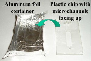
1. Put your chip with microstructures facing up in an aluminium foil container [1].
2. Pour a 2-3mm thick PDMS layer on top of the chip and cure it. A vacuum might be needed to remove the bubbles in the PDMS, if your features are small.
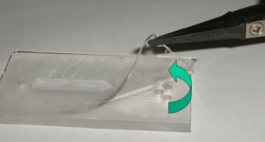
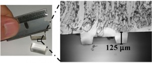
3. Peel off the PDMS and cut it at the location of your interest. Try to perform the cut under a stereomicroscope, if you feel it hard to locate your razor blade precisely.
4. Use the microscope to visualize the cross-section of the cut PDMS, and all the dimensions can be measured from the image.
References
[1] A. O’Neill, J. Soo Hoo and G. Walker, Rapid curing of PDMS for microfluidic applications, Chips & Tips (Lab on a Chip), 23 October 2006.


