Archive for 2015

A simple and inexpensive device to remove edge beads

Markus Ludwig and Seth Fraden

Martin A. Fisher School of Physics, Brandeis University, Waltham, Massachusetts 02454, United States

Why is this useful?


To achieve high resolution and high aspect ratio features in contact lithography it is necessary to have the photomask in direct contact with the photoresist during the exposure. This is impeded by the formation of edge beads on the edge of the wafer, which can measure multiples of the nominal resist thickness [1].

Dedicated spin coaters remove edge beads automatically just after spin coating. However, during soft baking, a new edge bead forms due to the coffee ring effect [2]. It is therefore recommended, especially for thicker resist films, to remove the edge bead not before, but after soft baking [3].

Edge bead removal is not critical on single layer devices. However, for multi level designs, edge bead removal can improve the feature resolution significantly. This is especially the case if the first layer of resist is thick and the second layer is thin.

This article presents the fabrication and use of a simple and inexpensive device to reliably remove edge beads by solvent spraying.

What do I need?


Materials:

  • 100 ml round media storage bottle GL45
  • Diba Labware bottle cap Q series GL45 2 x 1/4 -28 ports with valves (00945Q-2V)
  • acrylic sheet, 12” x 6”, 3/16” thick
  • polyethylene sheet, 1/16 “ thick
  • 3x AAA battery pack with on/off switch + batteries
  • Parker micro diaphragm pump T2-05 IC (3/32 ID)
  • 2x ¼-28 to barbed 3/32 ID fitting
  • silicone tubing  0.078” ID, 50 cm length
  • 2x flat head machine screw 4-40 3/8 + nuts
  • 2x socket head machine screw 6-32 3/8 + nuts + washers
  • stainless steel blunt needle with 27 gauge Luer polypropylene hub, 1/2″ length
  • cable tie 4”
  • polypropylene tube fitting, male Luer slip to barbed coupler, 3/32″ tube ID

Tools:

  • hot air gun (Aoyue 968a+)
  • laser cutter (40W/45W CO2 Hobby Laser by Full Spectrum Laser) or scroll saw, drill press and drill bits
  • soldering iron (Aoyue 968a+) and solder

What do I do?


To build the edge bead remover, first prepare all components as shown in figure 1.

Cut the acrylic sheet and the polypropylene sheet and drill the holes as indicated in the schematic1.pdf or schematic1.dwg (AutoCAD) file. Solder battery pack wires to the pump. Then follow the instructions in video 1.

Figure 1: Materials needed

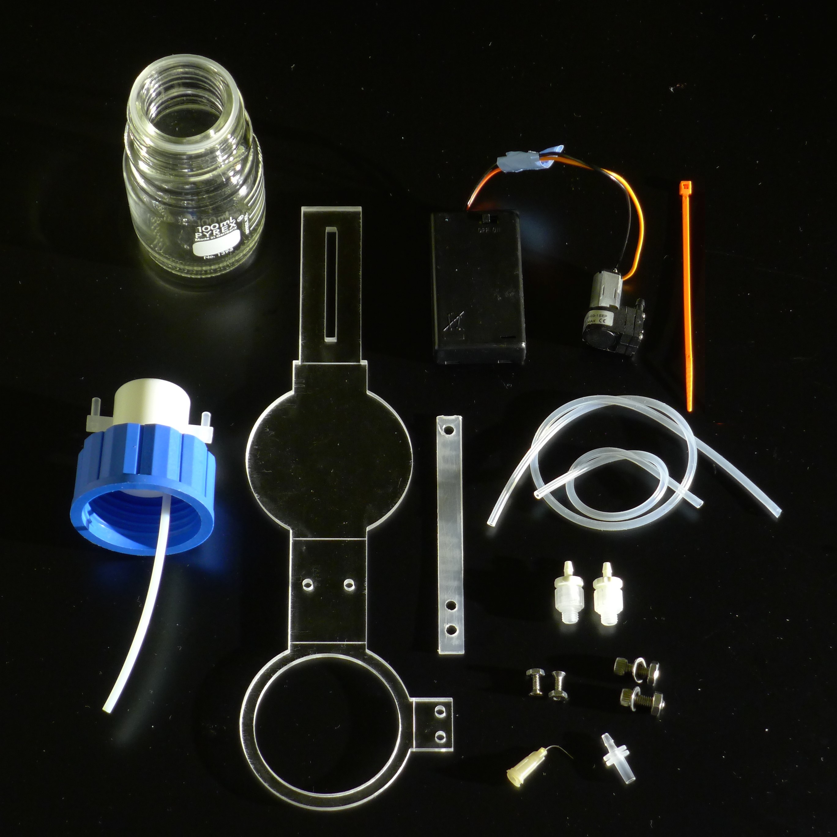
Figure 2: Assembled device

Edge bead removal (follow the instructions in video 2):

  1. Spin coat wafer, soft bake and cool down.
  2. Center the wafer on spin coater and spin at 700 rpm. The optional centering tool used in the video was 3D printed on a formlabs form one 3D printer. (Use centering tool.stl file to reprint)
  3. Turn on pump, open pump valve to pressurize bottle, position nozzle over edge bead.
  4. Open spray valve and dissolve edge bead
  5. Sweep outwards slowly and keep spraying for another 15 seconds.
  6. Turn off spray valve and ramp up to 2000 rpm for 10 sec.
  7. Turn off pump and close both valves. Developer may remain in the bottle and in the tubing.
  8. Wafer does not have to be baked again and can be exposed immediately.

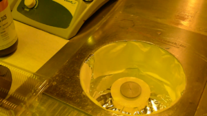
Figure 3: SU8 coated 3” wafer before (left) and after edge bead removal (right).

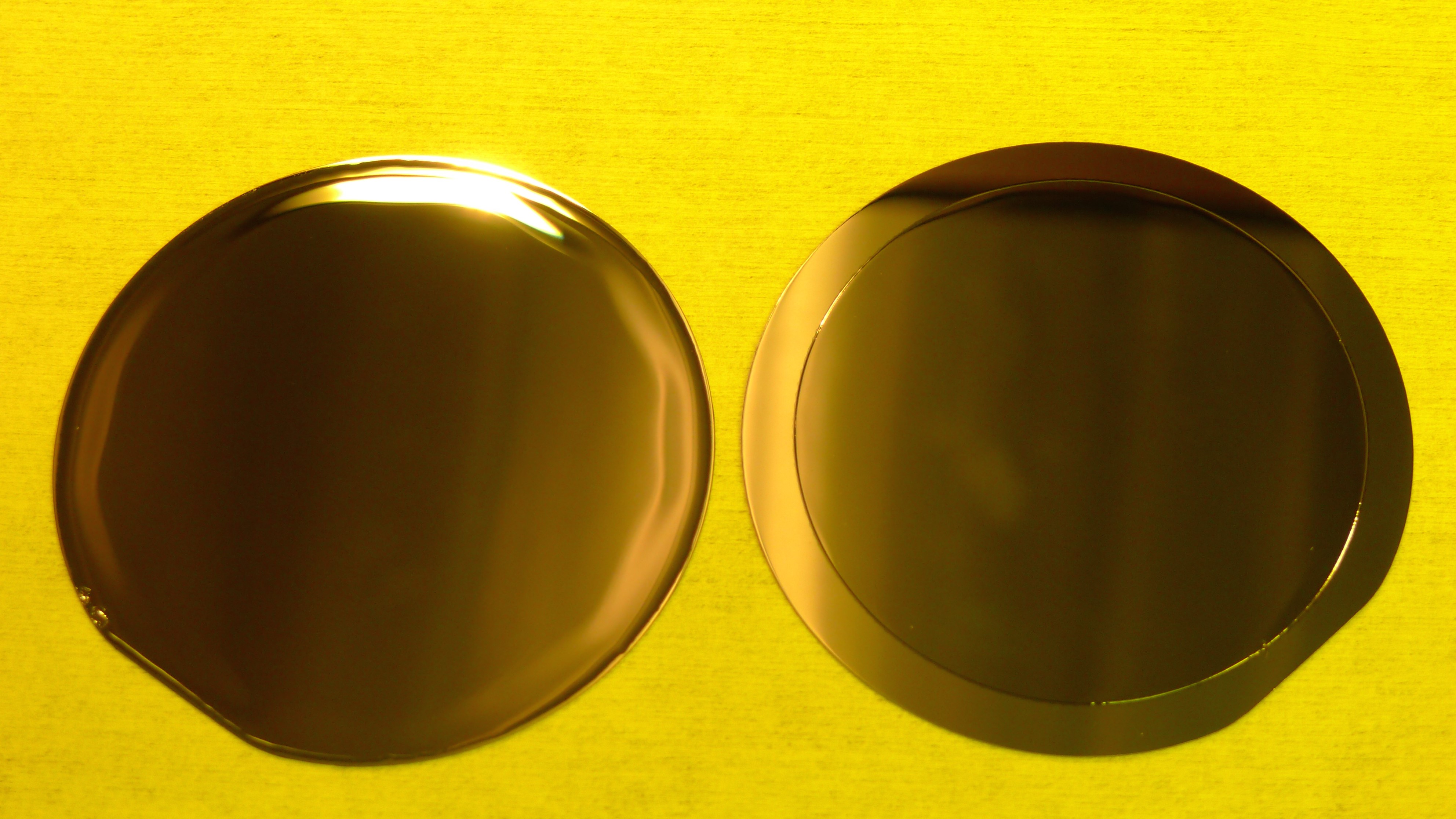
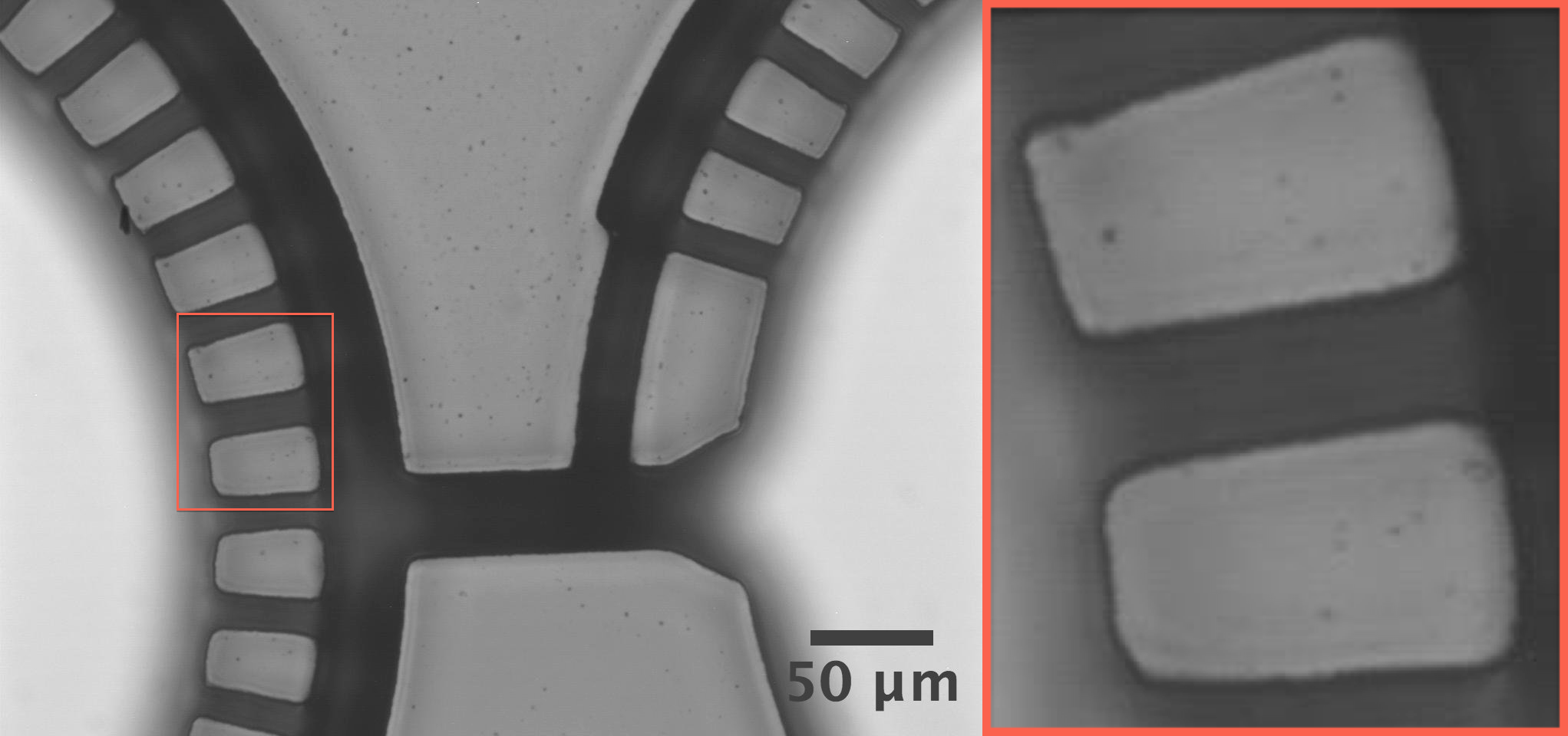
Figure 4: Comparison of feature resolution

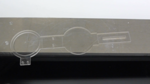
CAD drawing of a multi layer design

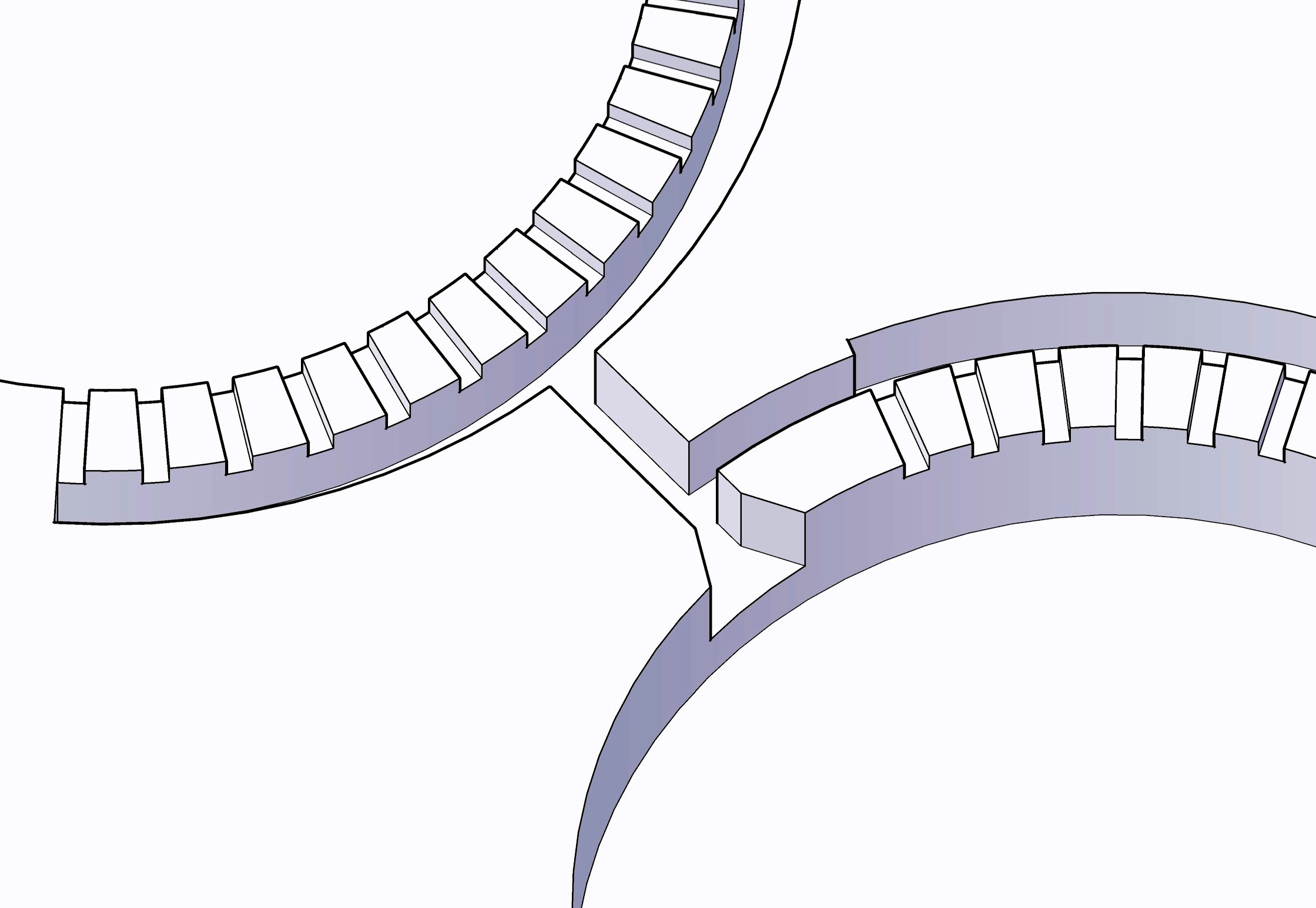
Figure 5: SU8 master fabricated with edge bead

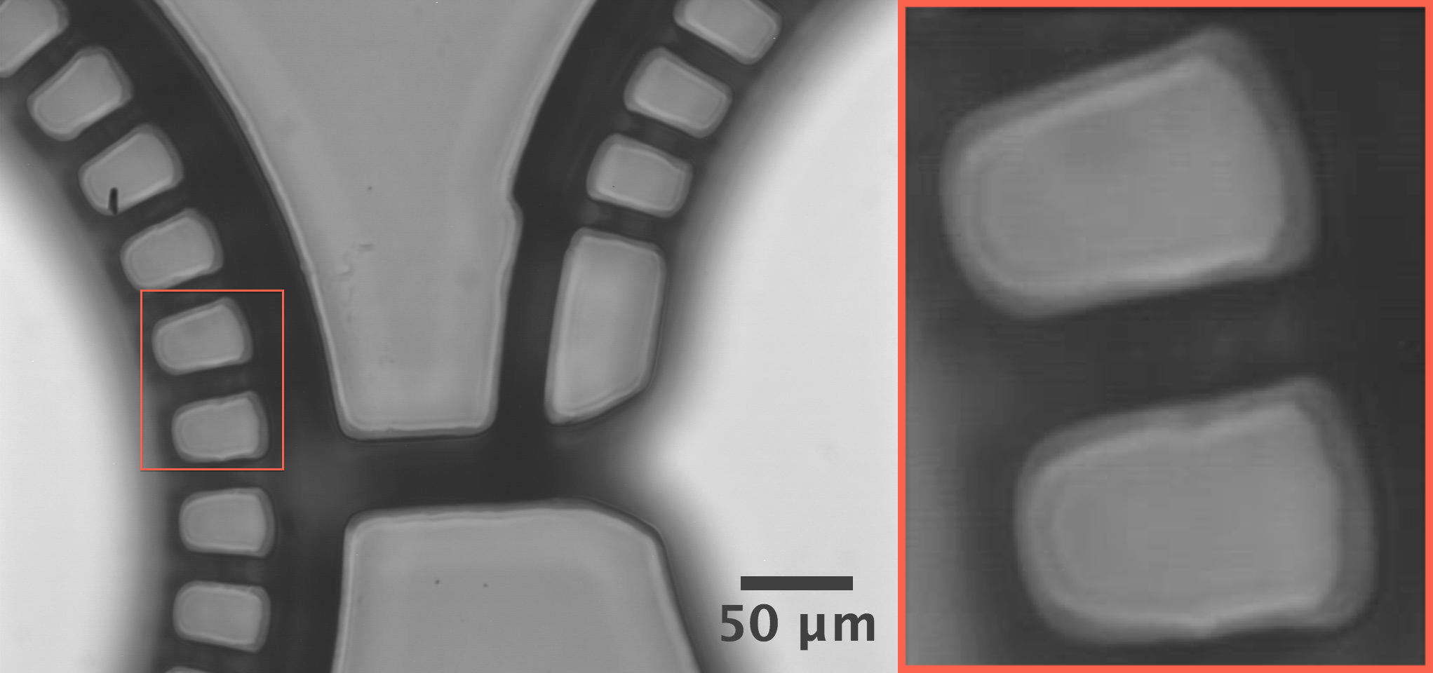
Figure 6: SU8 master fabricated without edge bead

Video 1:

Video 2:

References


[1] ‪ Shaurya Prakash, Junghoon Yeom, Nanofluidics and Microfluidics: Systems and Applications ‪Micro and Nano Technologies‪, William Andrew, 2014

[2] Robert D. Deegan, Olgica Bakajin, Todd F. Dupont, Greb Huber, Sidney R. Nagel and Thomas A. Witten, Capillary flow as the cause of ring stains from dried liquid drops, Nature 389, 827-829 (23 October 1997), doi :10.1038/39827

[3] http://www.cns.fas.harvard.edu/facilities/docs/SOP031_r2_6_SU-8%20photolithography%20process.pdf

Digg This
Reddit This
Stumble Now!
Share on Facebook
Bookmark this on Delicious
Share on LinkedIn
Bookmark this on Technorati
Post on Twitter
Google Buzz (aka. Google Reader)

A simple and low cost method to fabricate NOA microfluidic chips

Gabriele Pitingolo1, Raffaele Vecchione1,3 and Paolo A. Netti1,2,3

1 Center for Advanced Biomaterials for Healthcare, Istituto Italiano di tecnologia (IIT@CRIB), Largo Barsanti e Matteucci, 53, 80125, Naples, Italy.

2 Dipartimento di Ingegneria Chimica, dei Materiali e della Produzione Industriale D.I.C.MA.P.I, Università di  Napoli  Federico II, Naples 80125, Italy.

3 Centro di Ricerca Interdipartimentale sui Biomateriali (CRIB), Università di Napoli Federico II, p.le Tecchio 80, Naples, 80125, Italy

Why is this useful?


Microfluidic chips are often made of silicon or glass which presents the drawbacks of being relatively expensive, time consuming and has limitations to the geometries that can be realized. PMMA is an optimal solution to overcome these aspects but it presents a low chemical resistance to organic solvents and aggressive chemicals

Norland Optical Adhesive 60 (“NOA60”) is a clear, colorless, liquid photopolymer that cures when exposed to ultraviolet light1. Surface bonding can be activated with light therefore monolithic and transparent devices especially useful for optical elements can be realized. In particular, the use of NOA 60 eliminates premixing, drying, or heat curing operations common to other optical adhesive systems. Curing time is a matter of minutes and is dependent upon the thickness applied and the energy of ultraviolet light available. Dupont and colleagues have recently developed a NOA microfluidic channel via a photolithography multistep method that presents a long time process2.

Here, we demonstrate the possibility to micromachine already cured NOA substrates by micromilling that is much easier and cheaper than photolithographic techniques for fabrication of microchannels or microstructures in general.  In addition, by micromilling it is possible to easily drill and make open channels in NOA substrates if needed. Also, in the case of microstructures on the two layers to be bonded if one layer presents microstructures with feature sizes below 25 micron and one substrate with feature sizes above this value then it is possible to prepare one substrate by photolithographic techniques and the other substrate by micromilling with following bonding, saving time and money.

What do I need?


  • Fully cured PDMS mold
  • Norland Optical Adhesive 60
  • UV light (E-Series Ultraviolet Hand Lamps)
  • Micromachining machine
  • Oxygen plasma machine
  • Clamp

What do I do?


1. Pour liquid photopolymer NOA into a preformed PDMS mold covering the entire surface (figure 1A). After a few minutes to stabilize the liquid polymer put the PDMS mold under UV light for 30 minutes at a  365 nm wavelength (fig.1B).

2. After the curing time, NOA substrate is ready to use; to fabricate a microfluidic chip two NOA substrates are prepared. NOA substrates are replicated onto flat PDMS surfaces exploiting the flexibility of the PDMS mold as shown in figures 2A and 2B.

3. Take the NOA substrate and mill a channel and related inlet/outlet holes using a micromilling machine (Minitech CNC Mini-Mill) (fig. 3A-3B), the certified positioning accuracy of the three-axis are 12″ / 300mm in x-axis, 9″ / 228mm in y-axis, and 9″ / 228mm in z-axis. To minimize the experimental uncertainty, the NOA substrates preformed in point 2 are smoothed before milling.

4. Prepare the NOA channel (clean with water and dry with an absorbent cloth) and  treat the channel and top layer by exposing to oxygen plasma for 60s, at a pressure less than 0.1 Torr and with a plasma power of 20 W (fig 4A). Clamp the two substrates and put the clamped channel under UV-light for 1 h finalizes the bonding process (fig 4B).

5. Your well-bonded NOA microfluidic chip (Figure 5) is now ready to use.


References

  1. https://www.norlandprod.com/literature/60tds.pdf
  2. E. P. Dupont, R. Luisier and M. A. M. Gijs, Microelectronic Engineering, 2010, 87, 1253-1255.
Digg This
Reddit This
Stumble Now!
Share on Facebook
Bookmark this on Delicious
Share on LinkedIn
Bookmark this on Technorati
Post on Twitter
Google Buzz (aka. Google Reader)