Jonathan Siegrist, Mary Amasia, and Marc Madou
Departments of Biomedical, Chemical, and Mechanical Engineering, University of California, Irvine, CA, 92697, USA
Why is this useful?
The fabrication and bonding of rapid-prototyped polymer-based microfluidic devices is of great interest. The emphasis is not only on the ability to produce large numbers of devices rapidly, but to perform fast design and test iterations. Here, we present a method for rapidly cutting thin plastic films into complex shapes, such that sophisticated 2.5-D microfluidic chips can be created. The plastic layers are bonded together using traditional, low-pressure thermal bonding to minimize channel deformation while achieving high bond strengths capable of withstanding high-pressure & temperature operations, such as polymerase chain reaction (PCR). The authors have found this method to be particularly amenable to fast design iterations, as one can easily go from a design on the computer screen to testing of a real part within 3 hours.
The method presented here of cutting plastic films using a commercially-available knife-based cutter/plotter avoids the use of traditional CNC milling, which can leave behind burrs and rough edges. While hot-embossing and laser machining can be superior alternatives to CNC milling, they are considerably more complex and expensive than the method presented here. Also, by using a computer-controlled cutter, obvious advantages are gained in terms of possible design complexity and reproducibility as compared to previous Tips [1, 2]. Finally, this cutting method can be used for many types of plastic films (< 400 um thick, depending on the machine being used) without the need for extensive optimization of cutting speeds or feed rates.
The use of thermal bonding allows for much higher bond strengths as compared to the use of pressure-sensitive adhesives or double-sided tapes, and also provides a large dynamic range in terms of the types of plastics that can be used. For example, thin films of either high glass-transition temperature (Tg) materials such as polycarbonate or low-Tg cyclic olefin copolymers can be used with this method, as compared to lamination methods that are limited to low Tg materials only [3].
What do I need?
- Hydraulic Thermal Press, ideally with a max. temperature of at least 200ºC and a max. pressure of at least 1 MPa (the device used here was an MTP-8 from Tetrahedron Associates, Inc., CA, USA)
- Computer-Controlled Cutter/Plotter (the device used here was a CE-2000 from Graphtec America, Inc., CA, USA)
- CAD software
- Bare Si Wafers, at least single-side polish
- Plastic Films (the films used here were polycarbonate from McMaster-Carr, CA, USA)
- Double-sided Tape (3M Scotch brand was used here)
- Aluminium Foil
- Tweezers
- Alignment Pins (optional)
- Oxygen Plasma System (optional)
What do I do?
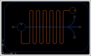
1. Design your microfluidic device using common CAD software (Fig. 1). Ensure the drawing for each layer is in a “polyline” format (i.e., each continuous line is defined as a single object) to facilitate smooth cutting. Import the CAD file into the software that controls the cutter/plotter.
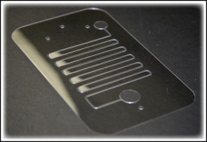
2. Attach your plastic film (using double-sided tape) to a plastic sheet that will act as your support/sacrificial layer (e.g., 0.75 mm thick). Place this structure in the cutter/plotter, and cut the film (Fig. 2). Cutting force and number of cuts may need to be optimized depending on the film thickness. We found that 2x low-force cuts worked well for 127 µm-thick polycarbonate films, and 4x medium-force cuts worked well for 254 µm-thick films.
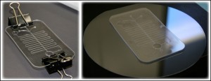
3. After all cuts are complete, carefully remove the part from the sacrificial layer and use tweezers to remove and discard the cut-out plastic features (Fig. 3). Repeat this for all layers, and then clean the plastic layers using isopropanol and water.
4. Align all of the layers, and hold together using a clip. You may include alignment pin features on your layers, and use pins to assist in alignment. For example, you could use 1 mm-diameter pins (McMaster-Carr, CA, USA – #91585A001).
5. Place the assembled microfluidic device layers on the mirror-finished side of a Si wafer, and remove the clip(s) (Fig. 4). Then place the second wafer mirror-finished side down on top of the microfluidic device, being careful not to disturb the alignment.
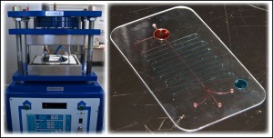
6. Place the assembly in the thermal press sandwiched between two pieces of foil, and thermally bond. Approximate parameters we found to work well for our proof-of-concept, multi-layer, polycarbonate device (1-top layer with loading/venting holes: 254 µm thick, 2-film with serpentine channel: 127 µm thick, 3-film with access holes and reservoirs: 127 µm thick, 4-film with linear channel: 127 µm thick, and 5-bottom layer: 254 µm thick) are shown in Fig. 5.
7. Remove the microfluidic device from the thermal press, and test (Fig. 6).
What else should I know?
Thermal bonding parameters, such as bonding temperature, pressure, dwell times, and ramping rates, will need to be optimized to ensure complete bonding of the plastic layers. The main disadvantage of thermal bonding is possible microchannel deformation, which can affect fluidic function. Thus, the Tg of your material, the number of layers, and the required bond strength will all need to be considered. The previous Tip on prevention of chamber-sagging has obvious uses here [4].
The limitations on feature size using this method should also be noted. The thickness (z-axis) of your channels/chambers is determined by the thickness of the films. We found the feature size (x-y plane) limitations when cutting films to be ~ 200 µm, as limited by the cutter/plotter being used. Newer machines list resolutions on the order of 10s of µm.
Finally, while these plastic parts are inherently hydrophobic, they can be made hydrophilic via oxygen-plasma treatment. Common plasma-treatment parameters for our devices are 200 W for 2 mins at 200 mTorr O2-pressure to provide hydrophilicity for many weeks. This can facilitate liquid loading and also serve as a sterilization step.
Acknowledgements
We would like to thank the DARPA-MF3 center for funding, and Dr. Albert Yee of UC Irvine for generously allowing us to use his thermal press.
References
[1] R. J. Holmes and N. J, Goddard, Rapid prototyping of microfluidics, Chips & Tips, (Lab on a Chip), 15 February 2007.
[2] R, Kumar, R. L. Smith, and M. G. Pappas, A method for rapid fabrication of microfluidic devices, Chips & Tips, (Lab on a Chip), 30 June 2009.
[3] D. Olivero and Z. Fan, Lamination of plastic microfluidic devices, Chips & Tips, (Lab on a Chip), 30 July 2008.
[4] J. Xu and D. Attinger, How to prevent sagging during the bonding or lamination of chips with large aspect ratio chambers, Chips & Tips, (Lab on a Chip), 24 July 2009.


