Javier Atencia and Laurie E. Locascio
Biochemical Science Division, National Institute of Standards and Technology
Why is this useful?
We present a simple method to bond glass wafers reversibly by recreating the bonding that occurs occasionally among glass slides coming from a new box. Typically, the bond is clear without fringes, indicating that the wafers are in close contact, and the bond is so strong that it is impossible to separate the slides with bare hands, though it is not permanent; the slides can be separated with a razor blade.
This type of bonding is called “optical contact” or “direct-bonding”[1] (Isaac Newton was the first to observe it) and has been used extensively in the past, primarily in the optical field.[2] It has also recently been proposed for microfluidic chips using two polished glass wafers.[3] Different protocols to induce optical bonding differ in the amount of labor and the bonding yield. The main advantages of this type of bonding include the following: the bond can be reversible; the method works with materials of different thermal expansion (it does not require heating); and the method does not require adhesive materials.
Here we introduce a simple, quick and reproducible realization of this type of bonding for microfluidic applications.
What do I need?
- Two polished 3″ circular wafers (surface roughness <5Å ), one of them with etched patterns on one side (there are many protocols in the literature) and through holes to access the patterns. (For other wafer geometries see the final section of this Tip.)
- A bath for piranha etching or RCA cleaning, and appropriate personal protective equipment.
- Cassette for 3″ wafers and a spin-dryer for wafers (if one is not available, see the final section of this Tip), e.g. Semitool-101.
- Two neodymium magnets.
What do I do?
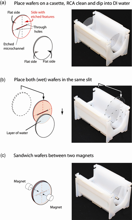
1. Place the glass wafers into different cassette slits (as usual), and place the cassette into the bath for RCA cleaning or Piranha cleaning (typically for 10 min.), Fig. 1(a).
2. Remove the cassette from the cleaning bath and place it in a bath of deionized water (for approx. 10 min.).
3. Remove the cassette from the deionized water bath, take one of the wafers out of its slit and place it into the same slit as the other wafer, taking care that the side of the wafer with the etched channels faces the other wafer. The two glass wafers should attach to each other by capillary forces and have a thin layer of water in between, Fig. 1(b). Care should be taken not to touch the sides of the wafers that will be in contact.
4. Carefully place two strong magnets on either side of the wafers that are in contact, thus sandwiching the wafers, Fig. 1(c). The magnets should be centered on the wafers.
5. Run the automatic protocol for spin-drying the wafers. The centrifugal force removes the liquid layer between the wafers, bringing them into close contact.
6. Remove the bonded wafers from the spin-dryer and remove the magnets. The microfluidic device is ready for use. (If the device will be used several hours later it is best to leave the magnets on the device until use.)
What else should I know?
Gas bubbles. Sometimes small gas bubbles may remain between the glass wafers after spinning. These bubbles can usually be removed by pressing on the glass wafers with your gloved fingers and driving them to the edges.
Reversible bond. If there are impurities such as small particulates between the wafers, the device will not bond well. In this case, a razor blade can be used to separate the wafers. Clean the wafers again and repeat the operation.
Bonding Strength. We tested this bonding method using glass microchannels (500 micrometers wide) with a lid made of glass (borofloat), and found that it withstood pressures of 207 kPa (30 PSI) consistently without rupture 24 h after spinning. We also tested a glass-sapphire and a glass-quartz bond and found that both consistently withstood pressures of 138 kPa (15 PSI).
Repeatability. We have used a device for months with this bonding without failure. We have also repeatedly separated the wafers with a razor blade, cleaned them, and bonded them again successfully for reuse.
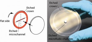
Surface quality. For this method to be successful, it is critical that the surface roughness is less than 5Å. If the wafers are not flat at the edges, etching a “crown” around the edges while etching the microchannels ensures proper bonding, see Fig. 2.
Aspect ratio of etched features. Because there is no thermal bonding, high aspect ratio devices can be fabricated without collapse of the features. For example, we created a circular chamber 500 nm deep and 1.5 mm in diameter, without collapse.
Temperature. We have used these devices at room temperature only, and expect them to fail if higher temperatures are employed due to thermal stresses – particularly when the device is made of two different materials.
No spin-dryer system or different wafer geometries
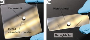
If a spin-dryer is not available, or if the wafers are different from each other or are not circular (see examples in Fig. 3), the same protocol can be used without spinning. However, in this case one should wait at least 24 h before using the device to allow the layer of water between the wafers to dry.
Acknowledgements
We are thankful to G. Cooksey for the photographs displayed in the figures.
Part of this work was performed at the NIST Center for Nanoscale Science and Technology Nanofab, which is partially sponsored by the NIST Office of Microelectronics.
References
[1] J. Haisma, N. Hattu, J. T. C. M. Pulles, E. Steding and J. C. G. Vervest, Appl. Opt., 2007, 46 , 6793-6803.
[2] V. Greco, F. Marchesini and G. Molesini, J. Opt. A: Pure Appl. Opt., 2001, 3, 85-88.
[3] Z. J. Jia, Q. Fang and Z. L. Fang, Anal. Chem., 2004, 76, 5597-5602.


