Archive for July, 2010

Wall plug inspired connectors for macro to microfluidic interfacing

Lorenzo Capretto1, Stefania Mazzitelli2, Stefano Focaroli2 and Claudio Nastruzzi2
1 School of Engineering Sciences, University of Southampton, UK
2 Department of Chemistry and Technology of Drugs, University of Perugia, Perugia, Italy

Why is this useful?


Common ways to link microdevices with standard fluidic equipments (such as syringe or peristaltic pumps) are based on the use of nanoports, created by: hand screwing a tube in the substrate material, gluing the tube fitting directly on the microfluidic device or commercial nanoports.
However, when such types of connection are used, there might be a series of potential issues, including: possible leakage of liquid from the connections, especially when high pressure inlet are required, possible clog of the port when glue is used or the high cost of the commercial devices.
Here, we demonstrate an easy and effective way for the creation of cheap and tight microfluidic connection ports for a varied range of substrate material including glass, silicon and polymers. Our approach solves the issues reported above with the creation of and inexpensive, well tight and glue-free port based on a “wall plug inspired” effect.

What do I need?


  • Plastic tube (ETEF, FEP or PTFE) 1/16″ OD, 0.75 mm ID [1]
  • 21 gauge hypodermic needle [2]
  • Drilling bit 1.5 mm [3]
  • A Proxxon, table top, micro miller [3] or any other handheld power tool
  • A cutting disc made of a hard abrasive [3] or any other tool for cutting the needle


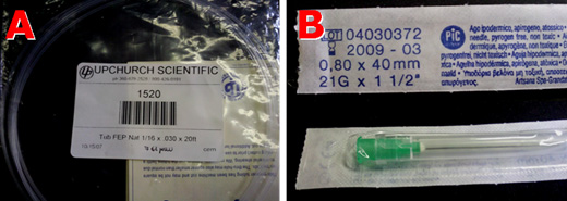
Fig. 1.  Tubing used for the production of “wall plug inspired” connectors for macro to microfluidic interfacing: FEP (fluorinated ethylene-propylene) tube (A) and hypodermic needle with Luer-Lock (21 gauge) (B).


Fig. 2. Stereo photomicrographs of the FEP tube (A), the hypodermic needle (B), the hypodermic needle inserted into the FEP tube (C) and the bit used for drilling the microfluidic chips (D). Note the different (crucial) sizes as determined by photomicrograph analysis. External diameter of the FEP tube: 1.58 mm (red arrow); internal diameter of the FEP tube: 0.76 mm (magenta arrow); external diameter of the 21 gauge needle: 0.82 mm (yellow arrow); external diameter of the FEP tube after insertion of the hypodermic needle: 1.66 mm and finally, diameter of the bit used for drilling the microchips: 1.5 mm (white arrow).

What do I do?


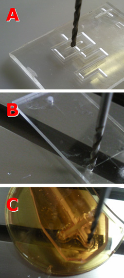
1. First drill the hole on the microfluidic device you wish to connect.


Fig. 3. Drilling process on different materials, namely: commercial TOPAS® COC (A) and custom made poly(methyl methacrylate) (PMMA) (B) or epoxy resin (C) chips.

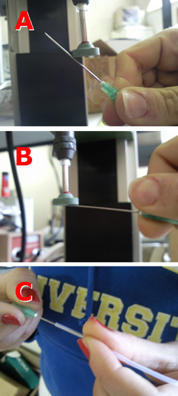
2. Cut the needle and pre-insert it in the plastic tube.


Fig. 4.  Assembly of the”wall plug inspired” connectors. Cutting (A), sanding (B) and insertion (C) of the needle into the FEP tube.

3. Assemble the port and tighten it in the previously drilled hole by inserting the needle in the tube. The needle must be inserted deeper than the interface between tube and hole in order to leverage the wall plug effect.


Fig. 5.  Insertion of the finished “spit inspired nanoport” into different chip type, namely: commercial TOPAS® COC (A) and custom made epoxy resin (B) or polydimethylsiloxane (PDMS) (C) chips


Fig. 6. Schematic representation of the assembling of “wall plug inspired” microfluidic ports.

References


[1] http://www.upchurch.com
[2] http://www.artsana.com
[3] http://www.proxxon.com

Digg This
Reddit This
Stumble Now!
Share on Facebook
Bookmark this on Delicious
Share on LinkedIn
Bookmark this on Technorati
Post on Twitter
Google Buzz (aka. Google Reader)

Chips and Tips – coming to this site shortly

Chips & Tips the free  – and unique, regularly updated forum for scientists in the miniaturisation field, will shortly be available on this new blog.   Chips & Tips provides a place where ideas and solutions can be exchanged on common practical problems encountered in the lab, which are seldom reported in the literature.

  • This new site will speed up publication of these valuable articles
  • Gives a more user-friendly interface
  • Allow you quicker access
  • Allow you to comment adding more tips
  • Allow wider sharing of articles across other social networking sites

Watch this space for new articles and sign up to the RSS feed from this site. I’d like to hear your feedback on how we can make the most of blogging technology to improve Chips & Tips, so please leave me a comment if you have  suggestions.

Read Chips & Tips on the old site.

Digg This
Reddit This
Stumble Now!
Share on Facebook
Bookmark this on Delicious
Share on LinkedIn
Bookmark this on Technorati
Post on Twitter
Google Buzz (aka. Google Reader)

Optimal protocol for moulding PDMS with a PDMS master

Jiaxing Wang1, Mingxin Zheng2, Wei Wang3,4*, and Zhihong Li3,4

1 Basic Medicine School, Peking University Health Science Center, Beijing, 100191, China
2 YuanPei College, Peking University, Beijing, 100871, China
3 Institute of Microelectronics, Peking University, Beijing, 100871, China
4 National Key Laboratory of Science and Technology on Micro/Nano Fabrication, Beijing, 100871, China
* E-mail: w.wang[at]pku.edu.cn

Why is this useful?


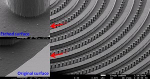
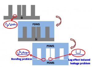
Nowadays, microfabricated silicon has been widely used as a master in PDMS-based soft lithography. It carries the merits of the microelectromechanical system (MEMS) technique, such as being able to construct complex 3D or high aspect ratio micro/nanostructures. However, the silicon master is easy to break during the PDMS moulding process. Due to the lag effects existed in deep reactive ion etching (DRIE) for silicon microfabrication, there will be a high risk of leakage between these two channels after PDMS moulding and bonding, if two parallel microchannels were designed too close, as shown in Fig. 1a. More seriously, the bonding surface of the PDMS replica will follow the morphology of the etched surface (Fig. 1a). Usually the etched silicon surface has high roughness, especially after a deep etching of silicon by DRIE (Fig. 1b), which makes the subsequent PDMS bonding being difficult, sometimes even impossible. To overcome the fragileness of the silicon master, it has been reported that moulding epoxy with PDMS replica, which is prepared by using the original microfabricated silicon as the master, to achieve a durable master in the PDMS moulding process. [1] However, this approach still suffers the aforementioned lag-induced leakage and bonding problems.

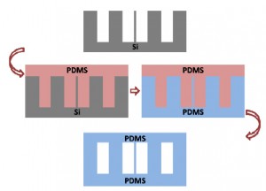
Moulding PDMS with a PDMS master replicated from the microfabricated silicon directly can overcome the aforementioned problems, as illustrated in Fig. 1c. It has been developed by silanizing the PDMS master with tridecafluoro- 1,1,2,2- tetrahydrooctyl- 1- trichlorosilane (in vacuo, 8h[2] or overnight[3]). In this Tip, we optimized the PDMS moulding process with the PDMS replica as the master. The optimal protocol is simple and easy to establish in any labs.
a

b

c

Fig. 1 Moulding PDMS with microfabricated silicon as master. (a) Schematic illustration of the lag effect induced leakage and bonding problems existed in the traditional soft-lithography when the PDMS is replicated from the microfabricated silicon master directly. (b) SEM photo of the microfabricated silicon master used in the present work (with the tilting angle of 45o). Inserted SEM photos give the morphology comparison between the etched silicon surface and the original one. (c) Schematic illustration of the moulding PDMS process with a PDMS master.

What do I need?


Microfabricated silicon, aluminum foil (Select HORECATM, Jinweiyuan Hotel Supplies Co. ltd.), mould release reagent (Micro90®, International Products Corporation, USA), PDMS (Sylgard 184; Dow Corning Co., MI), detergent (commercial available detergent, White CATTM, White Cat co. ltd.), ethanol (MOS grade, Beijing Chemical Reagent Institute).

What else should I know?


Process optimization

The present protocol contains two PDMS moulding processes: The first one is to construct the PDMS master from the microfabricated silicon while the second to make the final PDMS replica directly from the so-prepared PDMS master.

Considering the Corona-triggered PDMS-PDMS bonding technique [4], which will be adopted in the subsequent PDMS-microfluidic device construction, curing at 60oC for an hour of the PDMS pre-polymer prepared following the manufacture guideline was selected as the second PDMS moulding recipe. In this chips and tips, the first PDMS moulding process and the surface treatment of the PDMS master were optimized.

1) Optimization of the first PDMS moulding process
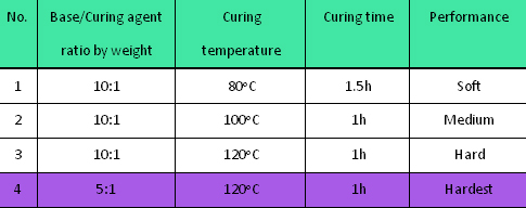
Table 1 Optimization of the first PDMS molding process

The first PDMS moulding process was optimized for the PDMS master preparation as shown in Table 1. Based on the above experiments, we found the optimal recipe for the first PDMS moulding process was curing the PDMS pre-polymer at 120oC for an hour with the mass ratio (Base to Curing agent) of 5:1. (Condition No.4)

2) Optimization of the surface treatment of the PDMS master

Table 2 Optimization of the surface treatment of the PDMS master

Surface treatment is another important factor for the PDMS moulding and was optimized as listed in Table 2. The results indicated that detergent dissolved in 75% ethanol (about 10 w.t.%) was the optimal recipe for the second PDMS moulding process. (Condition No.3) Herein, we name it the modified mold release agent. In later work we also use it for pre-treatment of the microfabricated silicon master.


How do I do it?


1. Make a holder with aluminium foil, according to the shape of the microfabricated silicon master. [5]
2. Mix the PDMS according to the manufacturer’s procedure, but with a mass ratio of the Base to the Curing agent of 5:1.
3. Pre-treat the microfabricated silicon master with the modified mold release agent.
4. Dry the microfabricated silicon master with nitrogen and put it into the holder.
5. Pour the PDMS pre-polymer into the holder, covering the whole microfarbicated silicon master, and then place the holder in an oven at 120oC for an hour.
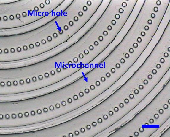
6. Gently peel the PDMS replica (the PDMS master in the second PDMS molding process) off from the microfabricated silicon master. (Fig.2)
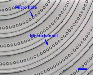
Fig. 2 The PDMS master, the PDMS replica from the microfabricated silicon. (The scale bar is 100μm.)

7. Treat the PDMS master with the modified mould release agent. For the deep holes (e.g. some holes with the depth of 100?m in Fig.2), treat the master with the modified mould release agent in the vacuum.
8. Place this PDMS master in a Petri dish, with the moulded-side upwards.
9. Mix PDMS prepolymer again according to the standard manufacturer’s procedure with a mass ratio of the base to the curing agent of 10:1.
10. Pour the PDMS mixture into the Petri dish, covering the whole PDMS master, and then cure at 60oC for an hour.
11. Carefully peel the PDMS replica (Fig.3) off from the PDMS master for the subsequent experiments.
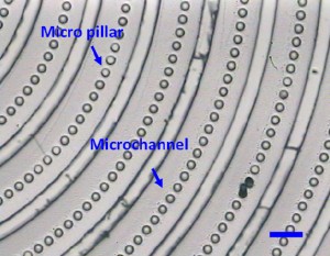
Fig. 3 The final PDMS replica from the PDMS master. (The scale bar is 100μm).

Acknowledgements


This work was financially supported by the 973 Program (Grant No. 2009CB320300).

References


[1] A. Estévez-Torres, A. Yamada and L. Wang,  An inexpensive and durable epoxy mould for PDMS, Chips & Tips (Lab on a Chip), 22 April 2009.
[2] J. R. Anderson, D. T. Chiu, R. J. Jackman, O. Cherniavskaya, J. C. McDonald, H. Wu, S. H. Whitesides and G. M. Whitesides, Fabrication of Topologically Complex Three-dimensional Microfluidic Systems in PDMS by Rapid Prototyping, Anal. Chem., 2000, 72, 3158-3164.
[3] J. L. Tan, J. Tien, D. M. Pirone, D. S. Gray, K. Bhadriraju, and C. S. Chen, Cells lying on a bed of microneedles: An approach to isolate mechanical force, Proc. Natl. Acad. Sci. U. S. A., 2003, 100(4), 1484-1489.
[4] C. Yang, W. Wang, and Z. Li, Optimization of Corona-triggered PDMS-PDMS Bonding Method, in Proceedings of the 4th IEEE International Conference on Nano/Micro Engineered and Molecular Systems, 319-322.
[5] A. O’Neill, J. Soo Hoo and G. Walker, Rapid curing of PDMS for microfluidic applications, Chips & Tips (Lab on a Chip), 23 October 2006.
Digg This
Reddit This
Stumble Now!
Share on Facebook
Bookmark this on Delicious
Share on LinkedIn
Bookmark this on Technorati
Post on Twitter
Google Buzz (aka. Google Reader)

A two-for-one dielectric and hydrophobic layer for digital microfluidics

Mais J. Jebrail, Nelson Lafreniere, Hao Yang and Aaron R. Wheeler
Department of Chemistry, University of Toronto, Ontario, Canada

Why is this useful?


Digital microfluidics (DMF) is a technique in which droplets of reagents in micro- to nano-liter volumes are manipulated by applying a series of electrical potentials to an array of electrodes[1]. In DMF devices, the actuation electrodes are coated with an insulating layer. Upon application of electrical potentials, charges accumulate on either side of the insulator, a phenomenon that can be exploited to make droplets move, merge, mix, split, and dispense from reservoirs. The insulating layer is covered by an additional hydrophobic coating, which reduces droplet sticking to the surface[2]. The instruments and materials required for forming these layers are expensive (tens-to-hundreds of thousands of dollars) and the deposition methods are time-consuming (many hours). We recently [3] demonstrated a new strategy for reusing DMF devices by fitting them with insulating polymer coverings (e.g., food wrap) that are spin-coated with Teflon. Here, we share an even simpler method that is cheap (tens of dollars) and fast (minutes)  featuring a two-for-one insulating and hydrophobic layer formed from laboratory wrap (Parafilm®, Alcan Packaging, Neenah, WI). No Teflon is required for fabricating these devices, and we speculate that this will be useful for laboratories interested in rapid prototyping for various applications.

What do I need?


  • Bottom substrate patterned with working electrodes (typically chromium or gold on glass); electrodes can be formed using conventional cleanroom techniques [4,5] or by rapid prototyping techniques such as microcontact printing [6], laser toner printing [7], or marker masking [8]
  • Indium-tin-oxide coated glass (can be purchased from Delta Technologies Ltd, Stillwater, MN) to serve as top substrate
  • Parafilm® and wax paper backing
  • Scissors
  • Scalpel
  • Hot plate

How do I do it?


1. With scissors, cut a piece of Parafilm® and stretch the film horizontally and vertically to its limits (a), and place over the bottom plate of the DMF device (with patterned electrodes) (b)

2. With a wax paper apply pressure with your finger on the film to release any air trapped between the electrode(s) and film (a). Then, score film with a scalpel and peel off excess Parafilm® (b,c).

3. Repeat steps 1 and 2 to apply parafilm layer to the top substrate (indium-tin oxide coated glass)
4. Place substrates on hotplate for 30 seconds at 80-85°C.
5. Allow substrates to cool down to room temperature (a), and then assemble the device with a top plate4,5 to dispense, merge and split droplets as shown in Figure (b-e).

What else should I know?


  • A ~4.5 x 4.5 cm piece of Parafilm® stretched to its limits will give a thickness of 6 – 9 mu.gifm.
  • A voltage of 300 – 500V is appropriate for actuation for above thickness.
  • Use of wax paper when applying pressure is important as it avoids contamination of Parafilm® surface.
  • Device can be recycled by simply peeling off old Parafilm® and replacing it with a new film.

References


[1] A. R. Wheeler, Science, 2008, 322, 539.
[2] J. Lee, H. Moon, J. Fowler, T. Schoellhammer, C. J. Kim, Sens. Actuator A-Phys., 2002, 95, 259.
[3] H. Yang, V. N. Luk, M. Abdelgawad, I. Barbulovic-Nad and A. R. Wheeer, Anal. Chem., 2009, 81, 1061.
[4] M. G. Pollack, A. D. Shenderov and R. B. Fair, Lab Chip, 2002, 2, 96.
[5] S. K. Cho, H. J. Moon and C. J. Kim, J. Microelectromech. Syst., 2003, 12, 70.
[6] M. W. L. Watson, M. Abdelgawad, G. Ye, N. Yonson, J. Trottier and A. R. Wheeler, Anal. Chem.,  2006, 78, 7877.
[7] M. Abdelgawad and A. R. Wheeler, Adv. Mater., 2007, 19, 133.
[8] M. Abdelgawad and A. R. Wheeler, Microfluid. Nanofluid., 2008, 4, 349.

Digg This
Reddit This
Stumble Now!
Share on Facebook
Bookmark this on Delicious
Share on LinkedIn
Bookmark this on Technorati
Post on Twitter
Google Buzz (aka. Google Reader)