Recently, the 50th anniversary of Moore’s law has been celebrated by the semiconductor industry. Although the current ITRS (International Technology Roadmap for Semiconductors) continues to propose “traditional” transistor materials such as Si and GaAs, attractive, two-dimensional alternatives have become visible on the horizon.
Schwierz et al. have recently published a Feature article in Nanoscale compiling the current knowledge on 2D materials. Their article focuses on the application of these as the channel material in field effect transistors.
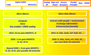
According to the authors, two large trends can currently be observed: More Moore and More than Moore. The former utilizes well known semiconductors and improves performance by sophisticated manufacturing and scaling techniques. In contrast, the latter one employs compound semiconductors and novel alloys as 2D materials with a wide range of new properties.
Two-dimensional materials and their prospects in transistor electronics
The main material classes researched to date are explained further, covering X-anes, Fluoro-X-enes, TMDs (transition metal–chalcogen combinations), SMCs (semimetal–chalcogen combinations), MX-enes and (currently theoretical) group IV-IV and III-V 2D materials.
To assess the viability of the materials for applications within electronic circuits, Schwierz et al. also describe a wish list of ideal properties of next generation channel materials: bandgap, carrier mobility, heat conductivity, contact resistance and scale length. Based on experiences from established semiconductors, they also derive practical values needed for high performance FET.
The final part of the review examines the current status of the material classes. Notable performance records of well researched materials (e.g. 100 GHz graphene FET) as well as first demonstrators (e.g. first X-ane based FET) are given here. Finally, some arguments for a revival of silicon as a promising material for future applications are also given.
Two-dimensional materials and their prospects in transistor electronics
F. Schwierz, J. Pezoldt and R. Granzner
Nanoscale, 2015, 7, 8261-8283. DOI: 10.1039/C5NR01052G
Sebastian Axmann is a guest web-writer for the Nanoscale blog. His interests comprise manufacturing and metrology of nanostructures as well as their usage in current semiconductor devices. He also posts links to interesting research articles on Twitter: @SebastianAxmann.


")