Archive for April, 2012

A refinement of a method to prevent sagging during the bonding or lamination of chips with high aspect ratio chambers

Brian Miller, Stewart Smith and Helen Bridle*
School of Engineering, University of Edinburgh, 3.17 William Rankine Building, Kings Buildings, Edinburgh, EH9 3JL, UK
Email: h.bridle[at]ed.ac.uk

Why is this useful?


Jie Xu and Daniel Attinger previously described a method to prevent the sagging of high aspect ratio channels during bonding [1]. The method involves careful placement of salt crystals into the channel prior to bonding to create a supporting structure. A limitation of the technique is the depth of channels this method can be used on, which must be within the size range of the salt crystals (~100 μm).

Described here is a method that builds on this technique to allow salt structures to be created with much smaller surface profiles, down to between 25-35 μm maximum heights of profile. This will allow the technique to be applied to shallower channels for devices in which performance is sensitive to channel height, for example, inertial focusing devices (Fig.1) [2,3].

This refined technique also helps to simplify the handling of the devices after preparation; reducing the risk of contamination of equipment as, once they are applied, the salt crystals are adhered to the surface of the device.

Inertial focusing devices
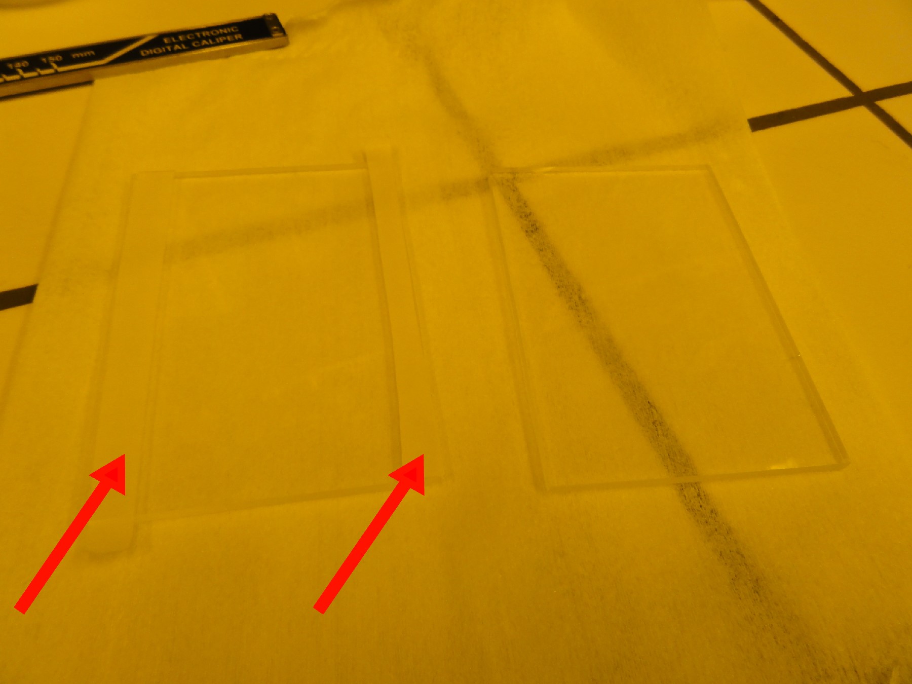
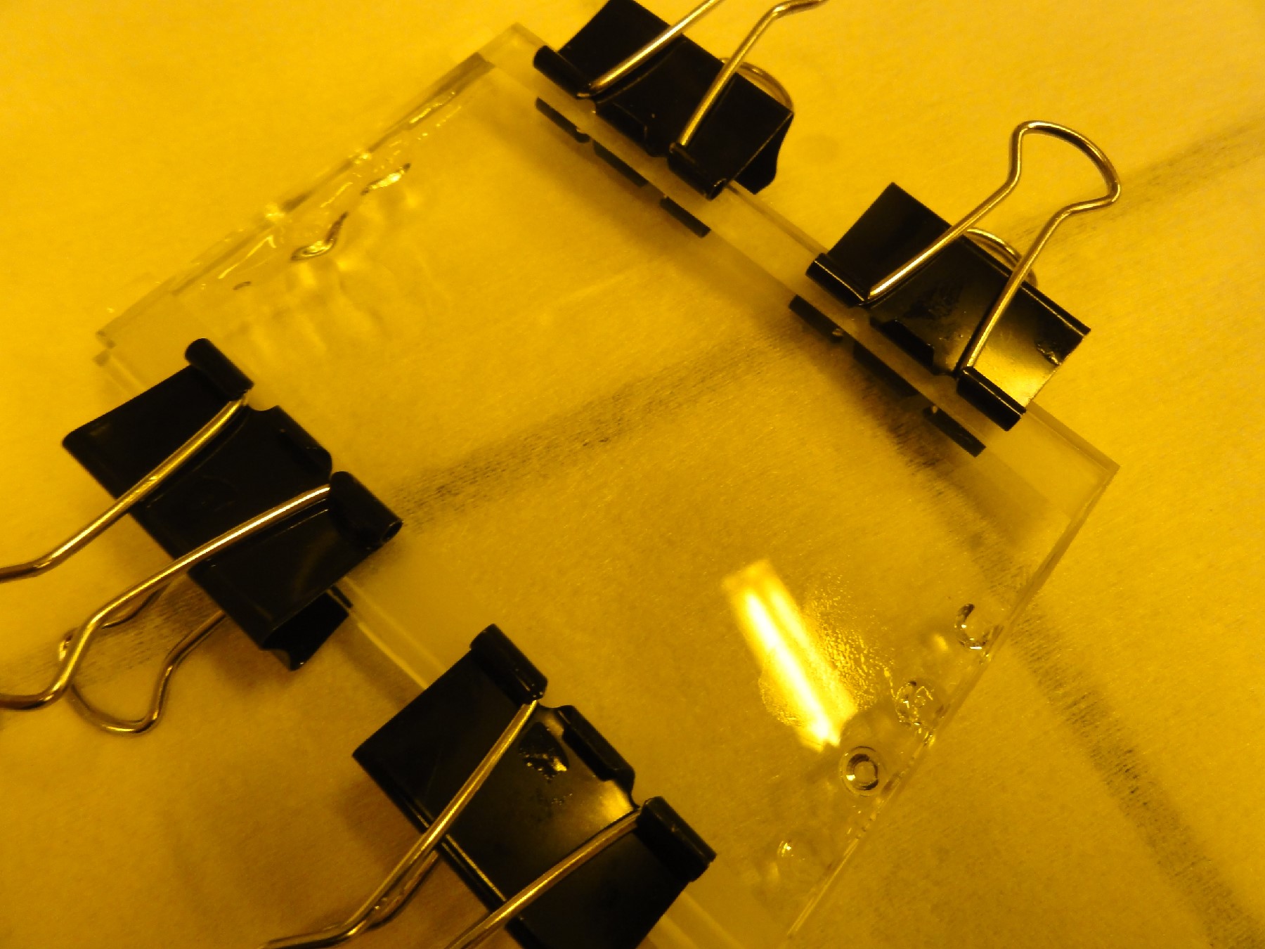
Figure 1. Inertial focusing device A; with solution applied to high aspect-ratio sections as indicated in pinched-flow segment B and output leg C. Device depth is 30μm (max. aspect ratio 60:1 in PDMS)

What do I need?


  • High purity KCl (potassium chloride salt)
  • De-ionised (DI) or reverse osmosis (RO) water
  • Weighing balances/scales
  • Decon 90 surfactant
  • Hypodermic needle (thin gauge)
  • Magnetic stirrer
  • Beaker and syringe

What do I do?


  1. Prepare a solution of the salt and surfactant by measuring 100ml of DI or RO water into the beaker. Add 1.5g of KCl to the water and stir gently for two minutes. Use the syringe to add 5ml of Decon 90 to the solution and stir very gently for a further two minutes, taking care not to foam the solution. Do not allow the solution to rest for more than a few minutes after stirring.
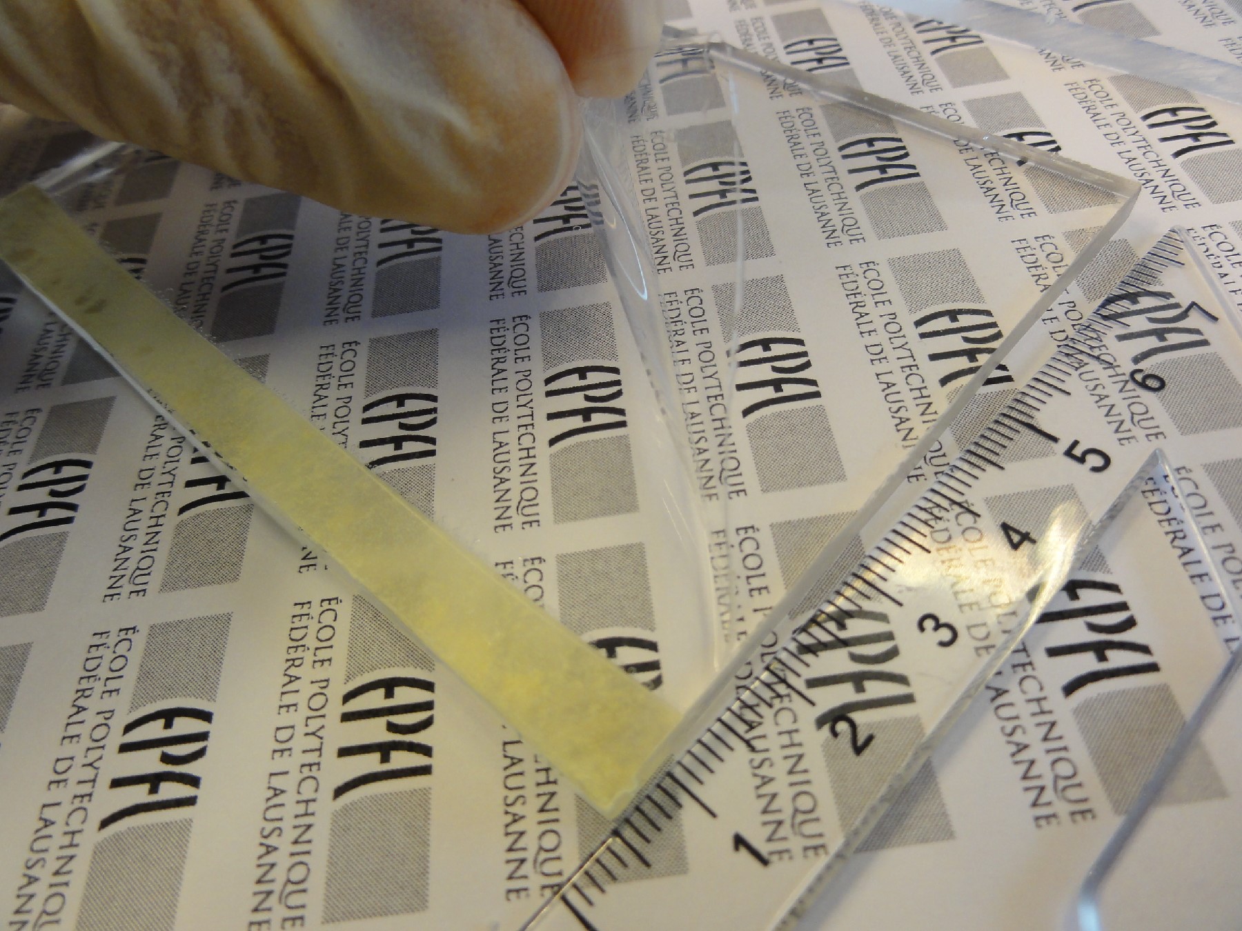
  2. Bending the sharp point of the hypodermic needle on your workbench or other hard, clean surface can help to ‘grab’ sufficiently small quantities of solution from the beaker. Use the needle or a similar applicator to carefully apply a small quantity of solution to the high aspect ratio section of your channel (Fig. 2). Only a very small volume is required and it is important to not allow the solution to overflow the channel. Dabbing the needle on a dust/lint-free wipe can help to regulate the amount of solution delivered to the surface of your device. If you accidentally over-apply the solution, clean the device with DI/RO water and IPA, and re-attempt application once it has dried.
  3. Allow the solution to evaporate at room temperature without assistance of any kind (no added air-flow or heat). An area of crystal formation should form where the solution was applied. The edges of this area tend to grow larger due to the ‘Marangoni effect’. The edge will typically be a maximum of 30-35μm in height, with the centre of the area typically yielding crystal formations between 10 and 25μm tall (as measured on a surface profiler over 4 repetitions), which should suffice to prevent the unintended bonding of the ceiling to the floor of the channel.
  4. Bond your device to your substrate layer following your normal bonding procedure (we used oxygen plasma bonding of PDMS to a glass microscope slide in this example).
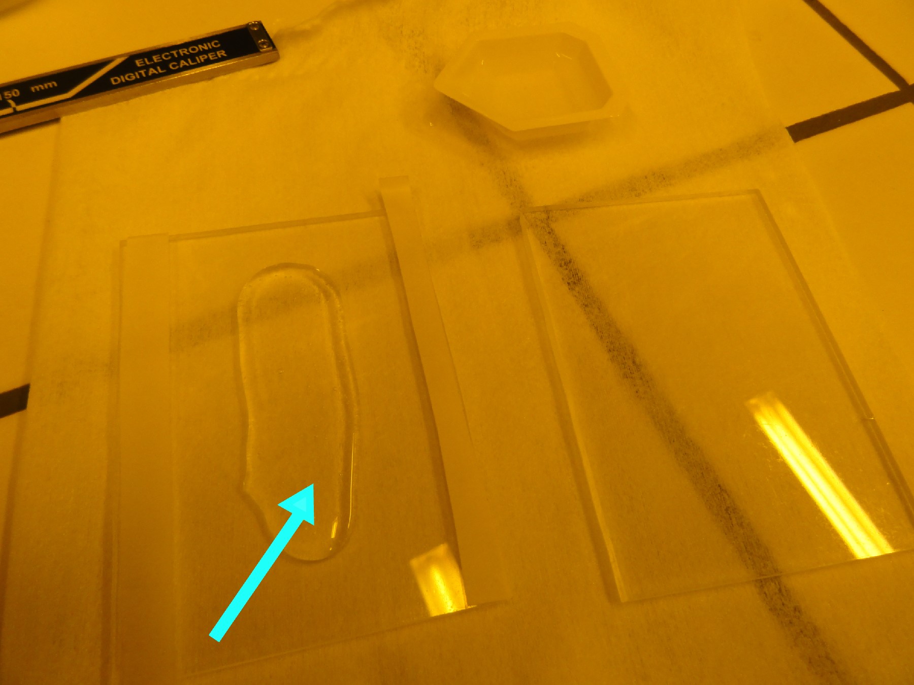
  5. Before using the device, run water or buffer through to dissolve away the crystal formations (Fig. 3). The surfactant helps to quickly remove the salt structures and leave the device clean of any remnants.

Application of solution into channels
Figure 2. Careful application of very small quantities of solution into channels, using a hypodermic needle

Support structures before and after rinsing
Figure 3. Top: water salt formations in the support structure before rinsing with DI/RO water. Bottom: the same area after rinsing through, illustrating that practically no residue is left in the device

Notes


  • Failure to use the surfactant will result in much larger crystal formations, as the crystal structures nucleate in very few locations and form much deeper structures. It is conjectured that the surfactant suspends the salt ions with a larger interspaced distribution throughout the solution, causing a much more distributed nucleation of the crystals and yielding the lower profile crystal formations.

References


[1]  Jie Xu and Daniel Attinger, How to prevent sagging during the bonding or lamination of chips with large aspect ratio chambers, Chips & Tips (Lab on a Chip), 24 July 2009.
[2] D. Di Carlo, D. Irimia, R. G. Tompkins and M. Toner, Continuous inertial focusing, ordering, and separation of particles in microchannels. Proc. Natl. Acad. Sci. U. S. A., 2007, 104, 18892-18897.
[2] D. Di Carlo, J. F. Edd, D. Irimia, R. G. Tompkins and M. Toner, Equilibrium separation and filtration of particles using differential inertial focusing. Anal. Chem., 2008, 80, 2204-2211.

Digg This
Reddit This
Stumble Now!
Share on Facebook
Bookmark this on Delicious
Share on LinkedIn
Bookmark this on Technorati
Post on Twitter
Google Buzz (aka. Google Reader)

Robust and easy macrofluidic connections in acrylic

Robert Henderson, Nick Selock and Dr. Govind Rao*
Center for Advanced Sensor Technology, and Department of Chemical, Biochemical, and Environmental Engineering, University of Maryland, Baltimore County, 1000 Hilltop Circle, Baltimore, MD 21250, USA
Email: grao[at]umbc.edu

Why is this useful?


The use of HPLC fittings and tubing in microfluidics is becoming more commonplace as the use of microfluidics in the sciences increases. Even though acrylic or PMMA is one of the most common plastic substrates used in microfluidics, the ability to strongly and easily connect an HPLC fitting to a PMMA chip has until now been elusive. Although there are some commercially available HPLC-to-chip products from Idex, they require heating the microfluidic chip well above the glass transition temperature of PMMA to create a permanent epoxy bond between attachment and chip. For these reasons, we present a simple scheme to strongly connect a standard HPLC flat bottom nut to a PMMA microfluidic device through the creation and bonding of an easy-to-make ¼-28 PMMA microfluidic union, using common lab equipment.

What do I need?


  • Laser cutter or another implement to cut PMMA, such as a hacksaw or band saw
  • An appropriate piece of equipment to anneal the PMMA (we use a convection toaster oven)
  • 5.3mm thick acrylic sheet for the body of the PMMA microfluidic union
  • A drill and drill bits
  • Vise grips, or another way to hold the PMMA union in place while tapping
  • A ¼-28 tap
  • A few sheets of progressively finer sandpaper
  • A 50-50% mixture of ethanol and water, along with an ultrasonic cleaner and lint-free wipes for cleaning purposes
  • A strong solvent for acrylic, such as chloroform or methylene chloride
  • A glass syringe with a blunt needle or needle blunted through filing

This connection scheme has been tested with good results when using the LT-115 and P-259 ¼-28 flat bottom HPLC nut and ferrule combination for 1/16″ OD tubing (Idex). This method was tested on microfluidic devices that were not bonded with the use of adhesives. This method is adaptable to other flat bottomed nuts as long as an appropriate tap and drill bit are used. Keep in mind that as the wall thickness of the PMMA union decreases, so does the strength of the connection between the HPLC nut and the device.

What do I do?


  1. Use a laser cutter to cut a circle with a diameter of 13mm out of the 5.3mm thick acrylic sheet. Make sure that you also either etch a center mark or make a small center hole using the laser cutter. If a laser cutter is not available, make a 13mm PMMA square using one of the other mentioned cutting implements. (Fig.1)
  2. Using a small drill bit, drill a pilot hole for the larger drill bit to follow in the center of the circle that you cut out in Step 1.
  3. Using the larger drill bit (a #3 or 0.213″ drill bit for the ¼-28 tap), drill the center hole in the cutout piece following the pilot hole drilled in Step 2.
  4. Using the ¼-28 tap and appropriate technique, tap the hole you have been creating in Steps 1-3. Do not use oil to lubricate the plastic as it is unnecessary and difficult to clean.
  5. After removing the plastic chips from the threads you just created, use progressively finer sandpaper to lap the surface that will make contact with your microfluidic device. Lapping the surface will ensure a very strong bond between the union and your device. We lap using a figure of eight motion to help guarantee a flat bonding surface. (Fig. 2)
  6. Anneal both your created microfluidic union and your device in an appropriate fashion. Annealing will relieve the thermal stress present in the union due to laser cutting and the drilling/tapping steps. (We use a convection toaster oven, set at 85ºC for 90 minutes, 50ºC for 30 minutes and then off with the oven door closed for 30 minutes. We find it useful to put a smooth metal plate below and above the piece to be annealed, to prevent uneven heating in the oven.)
  7. Thoroughly clean both the union and the microfluidic device to be bonded using a 50-50% mixture of ethanol and water. Clean only the union in an ultrasonic cleaner for 10 minutes. This mixture will not cause the union or the device to crack if they are both appropriately annealed beforehand and if the cleaning is performed within a few days of annealing.
  8. Place the union, lapped side down, onto the microfluidic device’s surface where the connection is desired. It is essential to center the union over the hole which receives the fluid or gas from the HPLC tubing. We use a small jig composed of two different sized plastic dowels to help us in this step (the black object in the bottom right corner of Fig.3).
  9. Pull some solvent into the glass syringe.While holding the union in place using your jig, gently drip some solvent from the glass syringe at the interface between the union and your microfluidic device (start with a single drop). The solvent will creep into the joint between the union you created and your microfluidic device due to capillary action. Add enough solvent to fill the gap between the union and your device, but be careful not to get any solvent into the fluid passages within your device.
  10. Being careful not to disturb the union’s position, gently apply pressure on the union until the surfaces become lightly bonded using your gloved fingers (Fig. 3). Light bond is usually achieved in less than a minute. In this step, also attempt to add enough pressure to force out any bubbles at the interface.
  11. Remove the alignment jig and add more solvent around the interface between the union and your device. This step reinforces the union’s connection to the microfluidic device.
  12. Put a small mass directly on top of the union, and leave the bonding union overnight to achieve the strongest connection between the union and your device.
  13. After the piece has dried overnight, remove the mass and then use the connection as you would any other flat bottom HPLC union. (Figure 4)

Raw PMMA union with laser centered hole
Figure 1. The dimensions of the raw PMMA union
Lapping the surface of the microfluidic device
Figure 2. Lapping the surface of the microfluidic device with a figure-eight motion
Bonding union and microfluidic device
Figure 3. Lightly bonding the union to the microfluidic device using gentle pressure
The finished microfluidic union
Figure 4. The finished microfluidic union

Notes


The following YouTube video ‘Power Tools & Carpentry Skills : How to Use a Tap & Die Set’ by Expert Village helps explain the use of taps (Step 4): http://www.youtube.com/watch?v=6DDhw191MLo

Acknowledgements


The authors would like to acknowledge the work of Dr. Yordan Kostov, Mike Tolosa and Mike Frizzell.

Digg This
Reddit This
Stumble Now!
Share on Facebook
Bookmark this on Delicious
Share on LinkedIn
Bookmark this on Technorati
Post on Twitter
Google Buzz (aka. Google Reader)

Easy and inexpensive fabrication of PDMS films of different thicknesses

Rodrigo Martinez-Duarte
Microsystems Laboratory (LMIS4), École Polytechnique Fédérale de Lausanne, Station 17, CH-1015 Lausanne, Switzerland

Why is this useful?


The following tip describes an easy and inexpensive way to fabricate PDMS films of different thicknesses. The main advantages are that no infrastructure (e.g. a spin coater) is needed for fabrication and that the materials needed are readily available. The idea here is to use a film of a specific thickness as spacer between two plates. PDMS is first deposited on one plate and squeezed in between plates to get a PDMS film with thickness similar to that of the film used as spacer. A similar methodology could be used to make films of other materials as well.

This methodology allows for very quick fabrication of a wide range of PDMS films using off the shelf components which are common in a traditional laboratory and office or can be easily purchased. The final goal is to fabricate films which feature different thicknesses, according to the original film used as spacer, and different hardnesses, by changing the ratio of PDMS to cross linker. The film can be stored and used as needed to cut off parts such as gaskets, spacers, etc. Here in the lab we use them to make microfluidic chambers of specific thickness.

What do I need?


  • 2 rigid plates with at least one flat surface per plate. They can be glass, PMMA (>3-4 mm thickness) or other material as long as they are rigid, preferably a fair thermal conductor and do not soften at temperatures up to 100°C. The use of transparent plates is not necessary but recommended to monitor the squeezing process of the PDMS and minimize the presence of bubbles in the final PDMS film
  • Pieces of a film, which can be tape, pieces of a plastic bag or any film that does not compress or  absorbs PDMS, with similar thickness to that being targeted for the PDMS film
  • Paper clamps, binder clips
  • General purpose soap or Mylar® film, the Mylar® film can be replaced by any film to which PDMS won’t adhere
  • And of course, PDMS and the equipment recommended to process it: balance, degasser and oven. Although this equipment is recommended, it is not necessary, as already suggested by Aung K. Soe and Saeid Nahavandi in a previous Tip [1]

Where do I get it and how much will it cost me?


In principle all the materials required are already available in the lab. The two plates can be two pieces of glass, as simple as two glass slides or two old wafers, or pieces of plastic, polycarbonate or PMMA for example. I have used PMMA plates and old glass wafers. The cost of the plates can be minimal and should not be more than $10. For example, you could go and buy a couple of very cheap picture frames with a glass piece of the size you want and use those. The pieces of film you use depend on the final thickness of the PDMS film and they can be obtained from a variety of sources, use your imagination! The paper clamps or binder clips are usually available in the office, if not you can buy them for several cents apiece.

What do I do?


  1. Wear gloves before starting. PDMS can be messy! The materials needed are detailed above and shown in Fig. 1.
  2. A. Dip your rigid plates in soapy water for a couple of minutes to deposit a layer that prevents PDMS from adhering to the plates. Remove the plates and blow them dry or let them dry naturally, do not wipe dry!
    Or alternatively:
    B. You may want to use a Mylar® film in between the rigid plate and PDMS. Take care not to scratch the Mylar® film. The rationale behind using this Mylar® film is to eliminate the need for surface treatment of your plates to prevent adhesion of the PDMS to them. PDMS does not stick to Mylar® and therefore you can easily just peel the Mylar® film off after you fabricate your PDMS film. A further advantage is that you don’t need to worry about scratching your plates or about cleaning the plates each time you use them. Storing your PDMS film between Mylar® films can also help protect it against scratches.
  3. Prepare your PDMS. Different ratios between the polymer and the cross-linker give different hardnesses. A 20:1 mix results in a gluey, soft film that easily sticks to a variety of materials. A traditional 10:1 results in a harder film. 5 grams of mix should be plenty for a couple of films featuring an area of 8 by 8 cm and thickness of up to 200 µm.
  4. A. If you treated the surface of the plates with soap: after the plates are dry (but still with the dried soap layer on them), you can position your spacer film close to the edges of the plate as shown in figure 2. Do this on only two edges to allow plenty of space for the PDMS to flow out from between the plates during step 7.
    B. If you are using the Mylar® films: cut the film into a couple of pieces similar to your plates. You can then position the spacer film close to the edges of one of the Mylar® films. Leave some space in between the spacer films to allow PDMS to flow out while pressing in step 7.
  5. After the PDMS is well mixed, manually deposit the PDMS mix on one plate treated with soap, or on the Mylar® film positioned on top of the plate, as shown in figure 3.
  6. Degas the previously deposited PDMS until the mix looks homogeneous (around 40 minutes in a general purpose degasser).
  7. Remove the arrangement from the degasser, place it on a flat surface and use the other plate to squeeze the PDMS in between the plates if you are using the soap-treating approach. If you are using the Mylar® films, then first lay the second film on top of the PDMS and then squeeze with the other plate. In both approaches, it is recommended to start applying pressure in one side and work your way towards the other side to avoid introducing bubbles in the PDMS.
  8. Use the paper clamps to clamp A) the plate-PDMS-plate or B) plate-Mylar®-PDMS- Mylar®-plate sandwich together at the location of the spacers as shown in figure 4.
  9. Bake for 1 hour at 80°C.
  10. Remove from oven and let cool for 5 min.
  11. A. If using soap: use a knife to remove the PDMS accumulated on the edges of the plates. This is important because it will facilitate the release of the PDMS film in the next step.
    B. If using Mylar® films: unclamp your sandwich and retrieve your PDMS film in between the Mylar® films. You are done!
  12. If using soap-treated plates: slowly but firmly separate the two plates, the PDMS film is likely to remain on one plate from where you can peel it off as shown in figure 5. Make sure you do it slowly to avoid rupturing the film. You may use fine tweezers to aid you during the release.
  13. You are done! You can store your film and later use a hole puncher, knife, etc. to cut off any feature you want.
  14. Clean the PDMS from your plates and store them clean for the next time. Avoid scratching the surface of your plates!

Notes


  • Tape (175, 140, 70 and 50 µm thick) and plastified paper (50 µm thick) have been used as spacers.
  • This methodology has been used to fabricate films as thin as 50-70 µm. The exact thickness of the PDMS film is difficult to measure due to the soft nature of the film.
  • The use of soap may interfere with further applications of the PDMS film. However, here in the lab we haven’t seen any adverse effects so far.

Fig.1 Materials needed: paper clamps, rigid plates and pieces of film (red arrows)

Figure 2. Pieces of film (red arrows) positioned close to the edges of the rigid plate shown on the left.

Figure 3. Manually deposited PDMS (blue arrow) on one of the plates

Figure 4. Squeezed PDMS between rigid plates using paper clamps

Figure 5. Release of the PDMS film from one of the plates after it has been cross-linked by heating

References


[1]  Aung K. Soe and Saeid Nahavandi, Degassing a PDMS mixture without a vacuum desiccator or a laboratory centrifuge and curing the PDMS chip in an ordinary kitchen oven, Chips & Tips (Lab on a Chip), 26 May 2011.

Digg This
Reddit This
Stumble Now!
Share on Facebook
Bookmark this on Delicious
Share on LinkedIn
Bookmark this on Technorati
Post on Twitter
Google Buzz (aka. Google Reader)

Fabricating microporous PDMS using a water-in-PDMS emulsion

Juyue Chena, Rui Zhangb and Wei Wang*a
a National Key Laboratory of Science and Technology on Micro/Nano Fabrication, Institute of Microelectronics, Peking University, Beijing 10871, P. R. China
b School of Pharmaceutical Sciences, Peking University, Beijing 10871, P. R. China

Why is this useful?


Microporous PDMS has been proposed as a functional PDMS material for cell culture related microfluidics applications where high gas perfusion is required to improve cell survival and functions. The phase separation micro-molding (PSμM) technique, which is widely used in microporous polymer preparation1, creates difficulties in fabricating microporous PDMS as there are many restrictions on the solvent – including high boiling point, low volatility, stability and appropriate compatibility with nonsolvent. Yuen reported that microporous PDMS can be simply prepared by curing PDMS pre-polymer with a porogen, such as salt or sugar particles, and then dissolving and washing away the porogen.2 However, it is difficult to obtain a microporous PDMS with pore size of micrometer scale by using this solid porogen. The small porogen makes the soaking and washing time cumbersome for most applications. As mentioned by Yuen, the porogen should be dissolved and washed away by soaking the PDMS and washing it in ethanol solution in an ultrasonic cleaner for at least 3 hours (longer may be required for smaller particles of porogen).

Fabrication of microporous PDMS

Figure 1. Fabrication of microporous PDMS by water-in-PDMS emulsion

Here, we propose a simple way to fabricate microporous PDMS using an emulsion of PDMS and water, as illustrated in  Figure 1. After manually blending the PDMS pre-polymer and water (1% SDS inside), water droplets were dispersed inside the PDMS pre-polymer. When the mixture is heated at a relatively low temperature (80oC) and in a relatively highly humid environment, the pre-polymer partially cures with the water droplets, keeping their original state. Through further curing at a higher temperature (120oC), the water trapped in the PDMS evaporates and leaves pores inside the PDMS matrix. Pore density is determined by the ratio of the water volume to the PDMS pre-polymer volume.

What do I need?


  • PDMS (Sylgard 184, Dow Corning Co.)
  • SDS (dodecyl sulfate sodium salt)
  • Deionised water
  • Petri dish
  • High temperature durable container
  • Oven

What do I do?


  1. Mix the PDMS according to the manufacturer’s instructions, with a mass ratio of base to curing agent of 10:1.
  2. Make the SDS solution, with a mass ratio of SDS to DI water of 1:100.
  3. Pour the PDMS pre-polymer and water (1% SDS inside) into a Petri dish with a given volume ratio, and manually blend them until a uniform emulsion (milky and opaque) is achieved. The water can be added step by step to facilitate the blending. Pore density is determined by the ratio of water volume to PDMS pre-polymer volume, as shown in Figure 2.

    SEM photos of microporous PDMS

    Figure 2. SEM photos of the prepared microporous PDMS. R = Vwater:VPDMS. (a) R = 0.01; (b) R = 0.05; (c) R = 0.3; (d) R = 0.7. All the scale bars represent 20μm

  4. Add some DI water in a high temperature durable container, and put the Petri dish with the water-in-PDMS emulsion inside on the water, then cover with the container lid. Put the container into the oven for about 2 hours at 80oC.
  5. Once the PDMS has been partially cured, remove the Petri dish from the container and finish curing it at a relatively high temperature in the oven for about 1 hour. After all the trapped water droplets have evaporated, the finished result is microporous PDMS.

References


[1] L. Vogelaar, R. G. H. Lammertink, J. N. Barsema, W. Nijdam, L. A. M. Bolhuis-Versteeg, C. J. M. van Rijn and M. Wessling, Phase separation micromolding: a new generic approach for microstructuring various materials, Small, 2005, 1, 645–655.
[2] P. K. Yuen, H. Su, V. N. Goral and K. A. Fink, Three-dimensional interconnected microporous poly(dimethylsiloxane) microfluidic devices, Lab Chip, 2011, 11, 1541-1544.

Digg This
Reddit This
Stumble Now!
Share on Facebook
Bookmark this on Delicious
Share on LinkedIn
Bookmark this on Technorati
Post on Twitter
Google Buzz (aka. Google Reader)

Simple and rapid fabrication of paper microfluidic devices utilizing Parafilm®

E. M. Dunfield, Y. Y. Wu, T. P. Remcho, M. T. Koesdjojo and V. T. Remcho
Department of Chemistry, Oregon State University, Corvallis, OR 97331, USA

Why is this useful?


Paper-based microfluidics offers several advantages over conventional microfluidics, and has great potential to generate inexpensive, easy-to-use, rapid and disposable diagnostic devices. Unlike traditional microfluidics, which often requires pumps to move fluid through the microfluidic channels, paper microfluidics can be performed without such instrumentation due to the flow of fluid being driven by capillary action through the paper. Hence, paper-microfluidics is well-suited for use in point-of-care diagnostics and in developing countries where expensive instrumentation is not available. There have been several advancements in the fabrication of paper microfluidic chips. Fabrication of paper-based chips can be done by photolithography [1], wax printing [2, 3], plasma etching [4], inkjet etching [5], and use of a cutting plotter [6]. However, such techniques may require the use of organic solvents during the fabrication process, they can be labor-intensive and expensive, and may impose limits on the types of materials that may be used in the chip. A novel technique is presented that utilizes a hydrophobic film material, Parafilm® “M”, which is heated to above its melting temperature of 60οC, and pressed into a piece of paper. The channel mask is cut from polycarbonate (PC) film, and sandwiched between the paper and the Parafilm®. The PC film mask prevents the melted Parafilm® from penetrating into the paper in the channel region, and therefore defines the hydrophobic boundaries of the paper channel. This technique has been tested on a wide variety of paper materials including Whatman Grade 1 filter paper, VWR light-duty tissue wipes and Kimtec Kimwipes, among other papers. While in some cases the paper can be cut directly into the desired channels, thin paper can easily tear and complex patterns proved to be challenging when cut by a cutting plotter. In contrast, the more rigid PC film can easily be cut into simple or complex patterns with a cutting plotter. Furthermore, the process is inexpensive, rapid, and does not require the use of organic solvents during fabrication.

What do I need?


  • Paper, such as Whatman filter paper, Kimtech Kimwipe or VWR light-duty tissue paper
  • Polycarbonate film, thickness approximately 100 µm
  • Parafilm® “M”
  • Aluminium foil
  • Scissors or x-y cutting plotter (for more complex channel patterns)
  • Hot press

What do I do?


  1. Cut out the desired channel patterns in polycarbonate film. For better cutting precision and accuracy, an x-y cutting plotter can be used.
  2. Create an assembly consisting of paper, polycarbonate (PC) cutout, and Parafilm® “M” as shown in figure 1. The paper can be Whatman filter paper, Kimtech Kimwipes, VWR light-duty tissue wipes or other paper of desired properties.

    Paper, polycarbonate and Parafilm® stack

    Figure 1. Paper, polycarbonate and Parafilm® stack set-up before heating and pressing.

  3. Cover both sides of the paper, PC, Parafilm® stack with aluminium foil to prevent sticking of the Parafilm® to the hot press plates, and place the whole assembly into the hot press.
  4. Heat the hot press to above 60οC, and apply ~200 psi of pressure for 1 minute. Note: 200 psi is necessary when using Whatman Grade 1 filter paper. Applied pressure varies depending on the thickness and porosity of the paper used.
  5. Allow the aluminium packet to cool, and then remove the foil from the paper microfluidic chip.

    Completed paper microfluidic chips made using Parafilm®

    Figure 2. Completed paper microfluidic chips made using Parafilm®. (a.) Spiral design has a channel width of 1 mm. (b.) Design has circles of 4mm diameter and 8 straight channels of 2mm width and 10mm length. (c.) Blue dye added to the paper microfluidics chip shown in b.

What else should I know?


For heavier weight paper such as Whatman Grade 1 filter paper, it is necessary to apply higher pressure (~200 psi) such as in a hot press to produce the microchips. However, for lighter weight paper such as Kimtech Kimwipes and VWR light-duty tissue wipes, microchips can simply be made by heating the plates of a heating element such as a hair straightener, and then applying gentle pressure to the paper, PC, Parafilm® stack to produce the paper-based chips.

References


[1]  A. W. Martinez, S. T. Phillips, B. J. Wiley, M. Gupta, and G. M. Whitesides, Lab Chip, 2008, 8, 2146-2150.
[2] Y. Lu, W. Shi, L. Jiang, J. Qin, B. Lin, Electrophoresis, 2009, 30, 1497-1500.
[3] E. Carrilho, A. W. Martinez, G. M. Whitesides, Anal. Chem., 2009, 81, 7091-7095.
[4] X. Li, J. Tian, T. Nguyen, W. Shen, Anal. Chem., 2008, 80, 9131-9134.
[5] K. Abe, K. Suzuki, D. Citterio, Anal. Chem., 2008, 80, 6928-6934.
[6] E. M. Fenton, M. R. Mascareñas, G. P. Lopez, S. S. Sibbett, ACS Appl. Mater. Interfaces, 2009, 1, 124-129.

Digg This
Reddit This
Stumble Now!
Share on Facebook
Bookmark this on Delicious
Share on LinkedIn
Bookmark this on Technorati
Post on Twitter
Google Buzz (aka. Google Reader)