Archive for the ‘Droplets’ Category

Manual Razor Patterned Tape Based Prototyping for Droplet Microfluidics

Saifullah Loneab* I. W. Cheongb and S. T. Thoroddsena

aDivision of physical Sciences and Engineering, King Abdullah University of Science & Technology, (KAUST), Thuwal, 23955-6900, Saudi Arabia.
bInstitute of Advanced Energy Technology, Kyungpook National University, Daegu, South Korea,
Phone: +821053165673, Office: +82-53-950-7590, FAX: +82-53-950-6594. Email: saifullah.lone@gmail.com, inwoocheong@gmail.com, and sigurdur.thoroddsen@kaust.edu.sa

Why is it Useful?

The subject of droplet microfluidics has grown in importance among researchers in chemistry, physics and biology, hence it has found applications in drug delivery, encapsulation, single-cell analysis, pickering-emulsion and phase-separation. For generating monodisperse droplets, various methods have been employed in constructing microfluidic devices. Emulsions with a coefficient of variation ≤ 5% have been previously reported in T-junction, flow focusing, co-axial, as well as other types of microfluidic devices. Microdroplets with ≤100 µm size offer attractive applications in industry and biology.  Small channel-diameters attained by clean-room soft lithography is the most precise technique for fabricating microfluidic devices.1, 2 This technique is widely used to make master molds for PDMS-based devices.3 However, regarding the cost and complexity, it is difficult to install clean-room soft lithography in financially challenged countries and laboratories. Therefore, the cost and special clean-room training restricts its wide-spread application. To develop low cost robust technologies; inkjet printing, controlled numerical machining, xurography or razor-writing, printed circuit technology, print-and-peel (PAP) microfabrication and 3-D printing have been tested to fabricate microfluidic devices without clean-room technology.  However, creating droplets under 100 µm size ranges by non-cleanroom technologies is challenging and open for upgradation. Recently, a rapid prototyping technique for microfluidics has been reported by employing laser-patterned tape4 This technique relies on computer-controlled CO2 laser beam. This work was further simplified by manual razor patterned tape-based prototyping for patterning mammalian cells.5 Building on this prototyping concept, we extended the idea to produce monodisperse droplets under 100 µm size rages by overlapping the razor patterned tape strips (at right angles) on a flat glass surface. The production of monodisperse emulsion under 100 µm size ranges are greatly useful in pharmaceutical and cosmetic industries. Hence, our approach may well serve as one of the simplest approaches to fabricate droplet microfluidic generators.

What do I need?   

  1. One-sided adhesive tape (Temflex 1500 electrical, thickness 150 µm)
  2. Flat glass slides, such as a microscope slide
  3. 30cm stainless steel metal ruler 
  4. Sharp razor blade
  5. Uncured mixture of PDMS base and curing agent (10:1 w/w)
  6. Oxygen plasma
  7. Oven or hot plate
  8. A microfluidic PDMS puncher for drilling holes
  9. Deionized water (D.I. water) and 20 cSt and 10 cSt silicone oil

What do I do?

Figure 1 outlines the prototyping procedure. Prototyping begins by attaching adhesive tape on a flat glass substrate. With a sharp razor-blade, the tape is cut into fine parallel strips. The thickness of the tape (150 µm) determines the depth of the microchannel, but this can be increased by attaching multiple layers of tape on top of each other. Next the tape is removed from the regions outside the fine strips.

To construct a cross-junction, one strip of the tape is lifted and horizontally placed on top of another at an angle of 90ᴼ. The junction is pressed gently to ensure the strips are well attached. These adhering strips of tape serve as a master for PDMS-based replica casting.

A mixture of PDMS silicone elastomer base and a curing agent (in 10:1 ratio) is poured on top of the master within a plastic petri dish. The mixture is degassed under vacuum for 1 h and cured for 4 hrs at 65°C. Cured PDMS replica is then cut and peeled-off from the master. The master can be used repeatedly to fabricate multiple copies of the PDMS replica by following the afore-mentioned steps. Inlet and outlet holes are drilled through PDMS replica, which is then bonded on a glass substrate, after both replica and glass has been exposed to oxygen plasma.  Figure 1(g) shows the resulting PDMS-device for generating monodisperse water-in-oil (W/O) emulsion. The technique is easily extended to fabricate T-junction or double T-junction prototypes (Figure 1h and i).

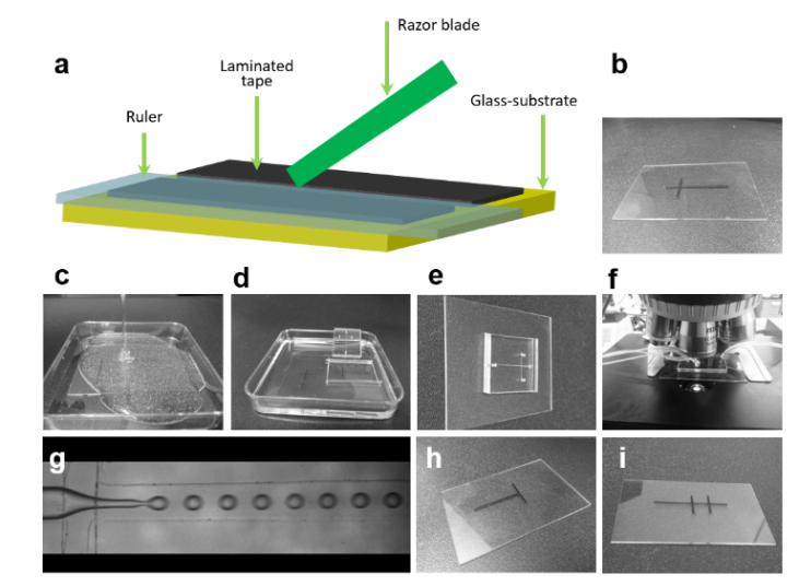
Figure 1. (a) Manual Razor Patterned Tape Based Prototyping for Droplet Microfluidics (b) Strips of adhesive tape on flat glass-substrate cut by a sharp razor-blade and a ruler, (c) The PDMS-casting, by pouring a mixture of PDMS silicone elastomer base and curing agent on top of the master in a plastic container. (d) Cut and peeled-off replica after curing. (e) Final assembled cross-junction microfluidic PDMS device. (f) Microfluidic device connected to syringe pumps under an optical microscope. (g)  Video frame showing water-in-oil droplet formation in a flow-focusing prototype. Panels (h) and (i) show razor patterned tape-based T-junction and double T-junction prototypes, respectively.
Figure 2. (a) Image sequence from a video recorded at 10 kfps showing water droplet formation at a cross-junction.  Time between subsequent frames is 200 µs.  (b) Droplet size as a function of capillary number based on the viscosity and flow-rate of the continuous-phase (20 cSt silicone oil), for the channel in panels (c) for 300 µm wide channel above the horizontal line and (d) for 150 µm channel below the horizontal line with 10 cSt silicone oil.  (c) Images extracted from video, showing flow regimes and droplet sizes as a function of flow-rate, with 300 µm channel width and 150 µm channel depth. (d) Video frame from smaller square channel with 150 µm width and depth.

Figure 2(a), demonstrates the droplet formation at a cross junction in our tape-based microfluidic device, with a channel width and depth of 300 µm and 150 µm respectively. In Figure 2(c), we kept the flow rate of aqueous phase fixed at 25 µl/min, while systematically increasing the flow-rate of outer continuous oil-phase (20 cSt silicone oil).  As the outer flow-rate is increased, the regime is found to shift from dripping at lower flow-rate to jetting at higher flow-rate (Figure 2(c)).  For lowest flow-rate, the aqueous-phase breaks into elongated plugs, while at higher flow-rates regular drops are pinched off.  Various factors affect the size of the droplets, but it is primarily determined by competition between viscous stress in the continuous phase Fv~ µU/d which tends to rip off the drop and the interfacial tension Fs ~ s/d which try to keep the drop attached. Here µ is the dynamic viscosity of the outer phase and U is its velocity; while s  is the interfacial tension between the water and the oil, s=0.040 N/m.  For small channels, the characteristic length-scale d is the same for the two forces and it therefore drops out of the balance and when Fv~ Fs then the non-dimensional capillary number Ca=µU/s characterizes their relative strength.  Figure 2b shows the droplet-size as a function of Ca.  When the flow-rate of oil-phase reaches 65 µl/min, the size of the droplets reaches ~100 µm and the droplet breakup occurs at a large distance from the cross-junction. Figure 2(d) shows drop formation with a channel width of 150 µm and a channel depth of 150 µm. In this case, the droplet size reaches down to ~73 µm, when the oil-phase (10 cSt) is flowing at 25 µl/min and aqueous-phase at 10 µl/min.


Acknowledgement: This work was jointly funded by King Abdullah university of Science & Technology (KAUST), Thuwal, Saudi Arabia , and the Ministry of Trade, Industry and Energy, Korea (Grants No. 10067082 and 10070241).


Reference

[1] Qin, D.; Xia, Y.; Whitesides, G. M. Rapid prototyping of complex structures with feature sizes larger than 20 μm. Adv. Mater. 1996, 8, 917-919.

[2] Xia, Y.; Whitesides, G. M. Soft Lithography. Angew. Chem. Int. Ed. 1998, 37 550- 575.

[3] Duffy, D. C.; McDonald, J. C.; Schueller, O. J.; Whitesides, G. M. Rapid Prototyping of Microfluidic Systems in Poly (dimethyl siloxane). Anal. Chem., 199870, 4974–4984.

[4] Luo, L. W.; Teo, C. Y T.; Ong, W. L.; Tang, K. C.; Cheow, L. F.; Yobas, L. Rapid prototyping of microfluidic systems using a laser-patterned tape J. Micromech. Microeng. 2007, 17 N107–N111

[5] Anil, B. S.; Ali, H.; Cheul, H. C.; and Raquel, P-C. Adhesive-tape soft lithography for patterning mammalian cells: application to wound-healing assays. BioTechniques, 2012, 53 315–318.

Digg This
Reddit This
Stumble Now!
Share on Facebook
Bookmark this on Delicious
Share on LinkedIn
Bookmark this on Technorati
Post on Twitter
Google Buzz (aka. Google Reader)

DMF Flip-Chips: an easy route to digital microfluidics

Steve C.C. Shih1, 2 and  Aaron R. Wheeler1, 2, 3
1 Institute for Biomaterials and Biomedical Engineering, University of Toronto, 164 College St., Toronto, ON, M5S 3G9
2 Donnelly Centre for Cellular and Biomolecular Research, 160 College St., Toronto, ON, M5S 3E1
3 Department of Chemistry, University of Toronto, 80 St George St., Toronto, ON, M5S 3H6

Why is this useful?


Digital microfluidics (DMF) is a technique in which discrete droplets are manipulated by applying electrical fields to an array of electrodes.1 An advantage of DMF is that droplets serve as discrete microvessels in which reactions can be carried out without cross-talk between samples or reagents. In contrast to the more conventional geometry of enclosed microchannels, each sample on a DMF device can be addressed individually, and reagents can be dispensed from reservoirs, moved, merged and split.2
A key component in a functioning DMF device is the insulating layer (i.e., a dielectric material) which is deposited on top of the actuation electrodes to facilitate the build-up of charge which drives droplet actuation.3 Fabrication of dielectric layers can be time-consuming and the costs for depositing them can be very expensive (e.g., a common method is chemical vapour deposition of parylene C).  Alternative methods have been described,4 but in all previous work, a separate dielectric layer must be positioned onto a device.

Here, we report a new method which we have called “DMF Flip-Chips,” in which the device substrate itself serves as the dielectric layer. In this method, actuation electrodes are patterned on one side of a glass coverslip (or other thin substrate), which is then flipped over such that the substrate serves as the insulating layer for droplet manipulation. This method is faster than conventional fabrication, and we speculate it will be useful for laboratories that do not have a dielectric coater but would like to use digital microfluidics.

What do I need?


  • Glass coverslips with thickness of 160 mu.gifm or less
  • Indium-tin-oxide coated glass (Delta Technologies Ltd, Stillwater, MN) to serve as top substrate
  • Scissors
  • Double-sided tape
  • Teflon-AF

How do I do it?


1. Pattern a glass coverslip with an array of electrodes. This can be accomplished using conventional cleanroom techniques2,3 or by rapid prototyping techniques such as microcontact printing,5 laser toner printing,6 or marker masking.7

Figure 1

2. Flip the substrate over and coat the “bottom” (now top) with Teflon-AF as described previously. Likewise, coat an ITO-glass substrate with Teflon-AF.2,3

Figure 2

3. Assemble the device with the patterned glass substrate on the bottom, double-sided tape spacers in the middle, and ITO-glass substrate on the top. Sandwich droplets between the two substrates.
4. Apply driving potentials (~500 VRMS and 15 kHz) between electrodes on the bottom and top plates, which causes droplets to a) dispense, b) move, c) merge, and d) mix as shown.

Figure 3

What else should I know?


  • Potentials of ~500 VRMS  are appropriate for bottom plates formed from a 160 mu.gifm coverslip.  Lower potentials can be used with thinner coverslips.
  • Additionally, lower voltages can be used for substrates formed from materials with higher dielectric constants than glass.
  • Clean surfaces with methanol or water after every use.
  • Thinner cover slips are difficult to use because they are very brittle and fragile.

Acknowledgements


We thank Irena Barbulovic-Nad for helpful discussions.

References


[1] A. R. Wheeler, Science, 2008, 322, 539-540.
[2] S. K. Cho, H. J. Moon and C. J. Kim, Journal of Microelectromechanical Systems, 2003, 12, 70-80.
[3] M. G. Pollack, A. D. Shenderov and R. B. Fair, Lab Chip, 2002, 2, 96-101.
[4] M. J. Jebrail, N. Lafreniere, H. Yang and A. R. Wheeler,  A two-for-one dielectric and hydrophobic layer for digital microfluidics, Chips & Tips (Lab on a Chip), 6 July 2010.
[5] M. W. Watson, M. Abdelgawad, G. Ye, N. Yonson, J. Trottier and A. R. Wheeler, Anal. Chem., 2006, 78, 7877-7885.
[6] M. Abdelgawad and A. R. Wheeler, Adv. Mat., 2007, 19, 133-137.
[7] M. Abdelgawad and A. R. Wheeler, Microfluid. Nanofluid., 2008, 4, 349-355.

Digg This
Reddit This
Stumble Now!
Share on Facebook
Bookmark this on Delicious
Share on LinkedIn
Bookmark this on Technorati
Post on Twitter
Google Buzz (aka. Google Reader)

A two-for-one dielectric and hydrophobic layer for digital microfluidics

Mais J. Jebrail, Nelson Lafreniere, Hao Yang and Aaron R. Wheeler
Department of Chemistry, University of Toronto, Ontario, Canada

Why is this useful?


Digital microfluidics (DMF) is a technique in which droplets of reagents in micro- to nano-liter volumes are manipulated by applying a series of electrical potentials to an array of electrodes[1]. In DMF devices, the actuation electrodes are coated with an insulating layer. Upon application of electrical potentials, charges accumulate on either side of the insulator, a phenomenon that can be exploited to make droplets move, merge, mix, split, and dispense from reservoirs. The insulating layer is covered by an additional hydrophobic coating, which reduces droplet sticking to the surface[2]. The instruments and materials required for forming these layers are expensive (tens-to-hundreds of thousands of dollars) and the deposition methods are time-consuming (many hours). We recently [3] demonstrated a new strategy for reusing DMF devices by fitting them with insulating polymer coverings (e.g., food wrap) that are spin-coated with Teflon. Here, we share an even simpler method that is cheap (tens of dollars) and fast (minutes)  featuring a two-for-one insulating and hydrophobic layer formed from laboratory wrap (Parafilm®, Alcan Packaging, Neenah, WI). No Teflon is required for fabricating these devices, and we speculate that this will be useful for laboratories interested in rapid prototyping for various applications.

What do I need?


  • Bottom substrate patterned with working electrodes (typically chromium or gold on glass); electrodes can be formed using conventional cleanroom techniques [4,5] or by rapid prototyping techniques such as microcontact printing [6], laser toner printing [7], or marker masking [8]
  • Indium-tin-oxide coated glass (can be purchased from Delta Technologies Ltd, Stillwater, MN) to serve as top substrate
  • Parafilm® and wax paper backing
  • Scissors
  • Scalpel
  • Hot plate

How do I do it?


1. With scissors, cut a piece of Parafilm® and stretch the film horizontally and vertically to its limits (a), and place over the bottom plate of the DMF device (with patterned electrodes) (b)

2. With a wax paper apply pressure with your finger on the film to release any air trapped between the electrode(s) and film (a). Then, score film with a scalpel and peel off excess Parafilm® (b,c).

3. Repeat steps 1 and 2 to apply parafilm layer to the top substrate (indium-tin oxide coated glass)
4. Place substrates on hotplate for 30 seconds at 80-85°C.
5. Allow substrates to cool down to room temperature (a), and then assemble the device with a top plate4,5 to dispense, merge and split droplets as shown in Figure (b-e).

What else should I know?


  • A ~4.5 x 4.5 cm piece of Parafilm® stretched to its limits will give a thickness of 6 – 9 mu.gifm.
  • A voltage of 300 – 500V is appropriate for actuation for above thickness.
  • Use of wax paper when applying pressure is important as it avoids contamination of Parafilm® surface.
  • Device can be recycled by simply peeling off old Parafilm® and replacing it with a new film.

References


[1] A. R. Wheeler, Science, 2008, 322, 539.
[2] J. Lee, H. Moon, J. Fowler, T. Schoellhammer, C. J. Kim, Sens. Actuator A-Phys., 2002, 95, 259.
[3] H. Yang, V. N. Luk, M. Abdelgawad, I. Barbulovic-Nad and A. R. Wheeer, Anal. Chem., 2009, 81, 1061.
[4] M. G. Pollack, A. D. Shenderov and R. B. Fair, Lab Chip, 2002, 2, 96.
[5] S. K. Cho, H. J. Moon and C. J. Kim, J. Microelectromech. Syst., 2003, 12, 70.
[6] M. W. L. Watson, M. Abdelgawad, G. Ye, N. Yonson, J. Trottier and A. R. Wheeler, Anal. Chem.,  2006, 78, 7877.
[7] M. Abdelgawad and A. R. Wheeler, Adv. Mater., 2007, 19, 133.
[8] M. Abdelgawad and A. R. Wheeler, Microfluid. Nanofluid., 2008, 4, 349.

Digg This
Reddit This
Stumble Now!
Share on Facebook
Bookmark this on Delicious
Share on LinkedIn
Bookmark this on Technorati
Post on Twitter
Google Buzz (aka. Google Reader)