Jonas M. Ribea, Nils R. Skovb, Ole-Andreas K. Kavlia, Armend G. Håtia, Henrik Bruusb and Bjørn T. Stokkea
a Department of Physics, Norwegian University of Science and Technology, NO–7491 Trondheim, Norway
b Department of Physics, Technical University of Denmark, DK–2800 Kongens Lyngby, Denmark
Why Is This Useful?
Contact angle measurements are important for characterizing the wettability of a liquid to a solid surface. In microfluidics they are of special interest as they provide insight into the intermolecular interactions between the sample liquid and the microchannel surface. Contact angle measurements are also important when assembling polydimethylsiloxane (PDMS) devices using oxygen plasma bonding. For optimal bond strength the water contact angle of plasma treated PDMS should be minimized as shown by Bhattacharya et al. [1] A current hurdle in measuring contact angles is the requirement of a setup that is expensive and non-portable. Here we show a method for measuring contact angles using materials and equipment found in a typical microfluidics lab.
What do I need?
Consumables:
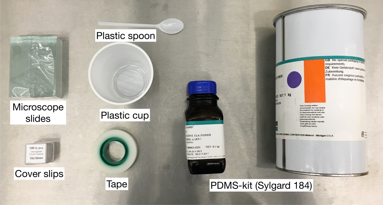
Equipment:
- Smartphone
- Digital scale
- Desiccator with vacuum pump
- Oven
- Syringe pump (optional)
- Light source
For measurements:
- Pipette (0.5–3μL)
- Sample (e.g. deionized (DI) water or other liquid sample)
What do I do?
Prepare PDMS:
- Weigh 10:1 PDMS (Sylgard 184) in a plastic cup on the digital scale
- Mix the PDMS by hand using a plastic spoon
- Degas the PDMS in a desiccator to remove the bubbles
Make PDMS-lens:
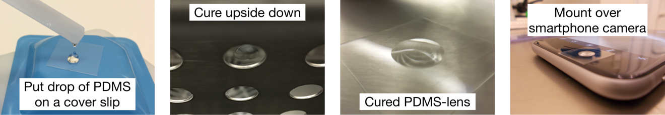
- Use the tip of the plastic spoon handle (or a pipette) to place a small droplet of uncured PDMS in the center of a glass cover slip. Repeat with various amounts of PDMS to obtain lenses with varying magnification.
- Mount the cover slips upside down (e.g. between two glass slides) and cure the PDMS hanging at 70 °C for 15 min. Longer curing times might be necessary, if the drop is relatively large.
- Center the PDMS-lens over the camera of your smartphone and fixate it using tape.
- Test the focus of your camera. For our camera setup the best images were captured with lenses that focus around 2 cm.
Contact angle measurements:
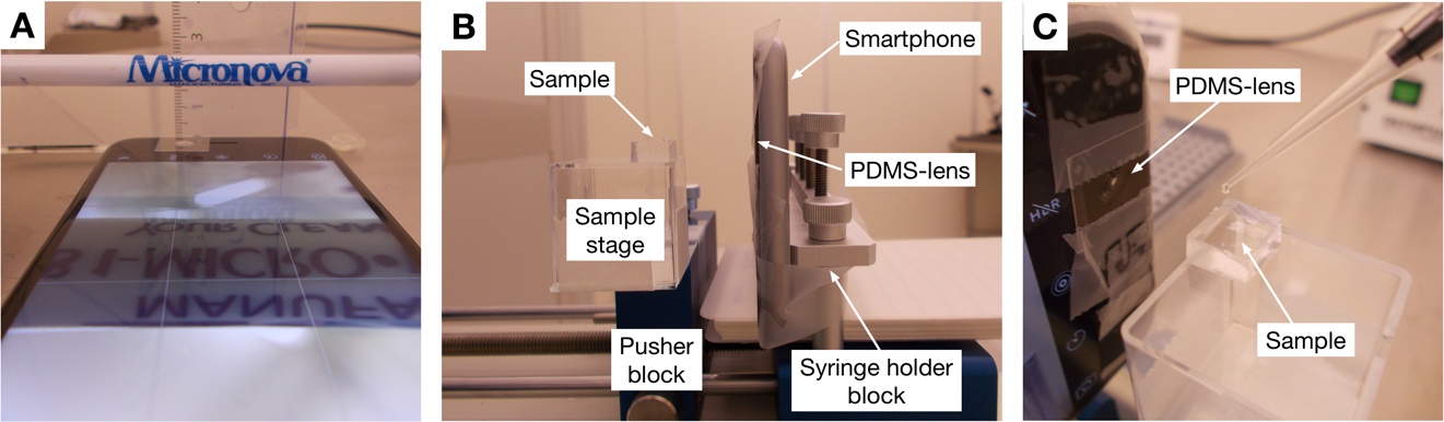
Smartphone contact-angle setup: (A) Focus test of a PDMS lens. (B-C) The smartphone mounted on a syringe pump. The PDMS-lens is mounted on the front facing camera of an iPhone 6S and the sample is centered in front of the lens. The sample is mounted on the pusher block of a syringe pump which can be moved to adjust the focus.
- Make a sample stage preferably using a syringe pump or some other system that you can move. We mounted the smartphone on the syringe holder block with the camera pointing towards the pusher block. Make a sample holder on the pusher block using glass slides or other consumables found in the lab. Align the center of the stage with the center of the camera. Tip: aligning is easier if done using the sample that you want to measure. Put the sample on the block and move it into focus by releasing the pusher block and sliding it away/towards the camera. Increase the height of the stage until the top of the sample is centered in the camera.
- Place the light source behind the sample and illuminate the stage evenly. Tip: put the sample stage in front of a white wall and light up the wall for a homogenous background and optimal contrast.
- Place a small drop (0.5–3 μL) of DI water on top of the sample using a pipette. Place the drop near the sample edge closest to the camera.
- Move the sample edge into focus. Block out ambient light in the room.
- Measure the contact angle of the drop in the image e.g. using ImageJ [2] software with a plugin for contact angle measurements [3] or get a rough estimate using an app on your smartphone.[4]
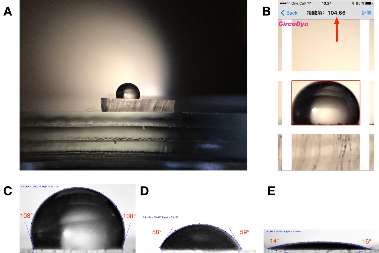
Contact angle measurements of water on PDMS: (A) Raw image from iPhone 6S front-facing camera with PDMS-lens. (B) Direct measurement using app on smartphone (based on θ/2 calculation) (C-E) ImageJ measurements using DropSnake plugin. Unmodified PDMS (C) and PDMS treated with oxygen plasma with increasing intensity (D-E).
What else should I know?
The focal length of the PDMS-lens is determined by the volume of PDMS used as described by Lee et al. [5]. However, it is difficult to control the volume of PDMS using a pipette due to the high viscosity of PDMS. We recommend making a range of lens sizes and testing them on your smartphone camera to see which gives the right focal length. If your digital scale has milligram precision you can measure the amount of PDMS used for each lens. The mass of each PDMS-lens is typically less than 10 mg. You can decrease the focal length further by adding PDMS to an already cured lens. Modern smartphones have both a rear-facing and a front-facing camera and in our experience the drop focusing was easier when using the front facing camera. The images taken here were captured with an iPhone 6S from Apple using the front-facing camera with a 5MP sensor. The weight of the cured PDMS lens was 7 mg.
Tip: you can also remove the PDMS-lens from the cover slip and place it directly on your camera. Although, it might be more difficult to center.
Calculating contact angles from images of sessile drops can be done using a range of techniques.[6] If the drop volume is small and the contact angles are not extreme, we can generally neglect droplet distortion due to gravitational effects. Extrand and Moon [7] calculated that gravitational effects can be neglected for a water droplet sitting on a hydrophilic surface (θ=5°) if its volume is less than 5 μL and less than 2.7 μL on a hydrophobic surface (θ=160°). If we assume the drop to be spherical, the contact angle can be estimated by multiplying the angle between the base and the height of the droplet by 2. This is referred to as the θ/2-method and is implemented by e.g. the Contact Angle Measurement app [4] for iOS. Sessile drop measurements are generally limited by the experimental setup and operator error, but typically has a precision of ±3°.[8] Image-processing algorithms relying on curve fitting of the droplet outline can enhance reproducibility. ImageJ [2] with DropSnake-plugin [3] uses active contours (energy minimization) to track the outline of the drop and calculate contact angles. This increases precision, but is slower and currently requires analysis on a separate computer.
Acknowledgements
The Research Council of Norway is acknowledged for the support to the Norwegian Micro- and Nanofabrication Facility, NorFab (197411/V30).
References
- S. Bhattacharya, A. Datta, J. M. Berg and S. Gangopadhyay, J. Microelectromech. S., 2005 14, 590–597
- ImageJ software
- DropSnake ImageJ-plugin for contact angle measurements
- Contact Angle Measurement iOS app (Japanese)
- W. M. Lee, A. Upadhya, P. J. Reece, and T. G. Phan, Biomed. Opt. Express, 2014, 5, 1626–1635
- Y. Yuan and T. R. Lee, Surface Science Techniques, Springer, Berlin/Heidelberg, 2013, 51, 3–34.
- C. W. Extrand and S. I. Moon, Langmuir, 2010, 26, 11815–11822.
- A.F. Stalder, G. Kulik, D. Sage, L. Barbieri and P. Hoffmann, Colloids and Surfaces A: Physicochem. Eng. Aspects, 2006, 286, 92–103.


")