Alexander Price, Wesley Cochrane and Brian Paegel Department of Chemistry, The Scripps Research Institute, Jupiter FL 33458
Why is this useful?
Syringe pumps are the most popular tool for transporting fluids within microfluidic devices. In the process of loading sample into a syringe, air bubbles (derived from the syringe dead volume) frequently migrate into the barrel and require removal to achieve consistent flow. Ideally, a researcher would have a large excess of sample so that the barrel can be filled and evacuated multiple times. During loading, syringes are held vertically with the sample directly below the tip, necessitating forceful evacuation to dislodge rising bubbles, however this not feasible for low/intermediate-volume “precious” samples (50-500 µL). Here, we present a simple funnel to aid bubble removal during syringe loading.
What do I need?
Plastic transfer pipets (FisherBrand 13-711-7M)
Razor blade
Pipette and pipette tips
Syringe (we use Hamilton Gastight 1700 series w/ TLL tips)
What do I do?
1. Using the razor blade, carefully cut the end off of the transfer pipet so that it fits snugly over the tip of your syringe (Fig. 1). It might take a couple tries, but you can use this as a template once you have found the right location to cut.
2. Cut the transfer pipette again, roughly 2 inches up from the previous cut (Fig. 1). Your funnel is complete.
3. Attach the funnel onto the tip of the syringe. Holding the syringe vertically (funnel up), load your sample into the bottom of the funnel (Fig. 2).
4. Fill and evacuate the syringe barrel as needed to eliminate any air bubbles (Fig. 3).
5. Dispose of the funnel.
Figure 1. Construction of a syringe funnel from a transfer pipet.
Figure 2. The funnel is attached to the syringe (left), and sample is loaded into the bottom of the funnel (middle and right).
Figure 3. Air bubbles in the barrel are expelled into the funnel and syringe is filled.
Comments Off on Syringe funnels for facile loading of precious samples
David J. Guckenberger,*aJake Kanack,*aLoren Stallcop,b David J. Beebea
aDepartment of Biomedical Engineering, Wisconsin Institutes for Medical Research, University of Wisconsin-Madison, Madison, WI, USA bDepartment of Materials Science and Engineering, University of Wisconsin –Madison, Madison, WI, USA * Authors contributed equally
Why is this useful?
With several microfabrication techniques now available, including: 3D-printing,1 micromilling,2 and hot embossing,3 in-house fabrication of thermoplastic microdevices has become cheaper, faster, and easier. However, for many applications – such as cell culture and microscopy – these devices must be bonded to optically-transparent substrates such as glass. While bonding similar materials, such as Polystyrene (PS) to PS, is relatively simple, bonding dissimilar materials, such as PS to glass, presents a particular challenge. Current methods to circumvent these challenges include spin coating adhesives, such as polydimethylsiloxane (PDMS), onto sacrificial substrates4 and injecting adhesive directly into the bond interface.5 However, equipment requirements, associate long cure times, heterogeneity in glue uniformity, and complexity limit acceptance of these techniques.
Here we present simple technique for applying uniform layers of adhesive to enable rapid – less than a minute – bonding of PS to glass. Using UV-curable adhesives, readily accessible materials, and a simple techniques, we demonstrate how to apply thin uniform layers of adhesive to a microchannel. We provide design suggestions that will improve bonding repeatability, and additional information that may help apply this technique to materials beyond PS and glass.
Adhesives are often material-specific. Consult the manufacturer to determine the best adhesive for your application.
Tip: Some adhesives may require post-treatment / aging to reach a full cure.
We have tested this protocol with Ultra Light-Weld 3025 (Dymax) and Norland Optical Adhesive 68 (Thor Labs, Inc.). These adhesives had similar performance, however the protocol may need to be tailored for other adhesives.
If the adhesive is too viscous or does not adequately wick around the rib, heat may be applied to achieve thinner adhesive layers, or to improve the wicking of the adhesive.
This protocol is amenable to wide variety of materials, including: cyclic olefin copolymer (COC), glass, metal, PS, and various rapid-prototyping materials.
Creating the rib and allowing the adhesive to wick eliminates excess adhesive and prevents adhesive from squeezing into the microchannel.
What do I do?
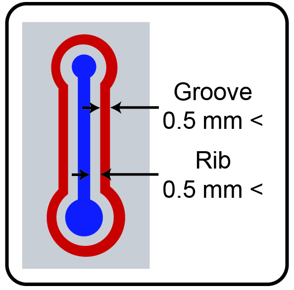
Fig.1 Channel border design
Step 1: Fabricate the microdevice. To improve bonding repeatability and adhesive distribution we recommend fabricating a groove (thickness > 0.5mm) around the channel – leaving a rib (0.5 mm < thickness < 1.5 mm) around the perimeter of the channel.
Tip: Rib thickness may need to be tuned for individual adhesives
Tip: Extra caution while applying the adhesive may be necessary for channels shallower than 0.1 mm
Step 2: Thoroughly clean the surface of the microdevice, silicone foam sheet, and coverslip using isopropyl alcohol and low-particulate wipers. Remaining particulates can be blown off with compressed air. Ensure PS and glass surfaces remain clean throughout the bonding process.
Step 3: Apply a dollop of UV curable adhesive to the foam sheet.
Step 4: Use a tongue depressor to spread the adhesive into a uniformly thin layer across the foam. The area of the adhesive should be larger than the microdevice – add more adhesive if necessary.
Step 5: Position the device onto the adhesive bonding surface down. Press down gently; avoid sliding the microdevice to prevent build-up of adhesive within the channels. Pick up the device and repeat this step two or three times to ensure the bonding surface is completely covered with adhesive.
Tip: Take care to ensure no adhesive is transferred from gloves to surfaces of the device not intended to be bonded.
Tip: Minimize the delay between step 4 and step 5 to help ensure a uniform thickness of adhesive
Step 6: Position the microdevice above the coverslip, and gently lower it until it makes contact. Once contact is made, release the device, taking extra caution to avoid sliding the microdevice.
Tip: The adhesive may have a yellow color after bonding. If necessary, allow 24 hours for adhesive to clear
Step 7: Allow a few seconds for the adhesive to wick along the ribs, then cure device for 20 seconds with ~350 nm UV light at [Intensity]
Fig. 2 Process workflow
What else should I know?
Fig. 3 Cross sectional image of a PS microchannel bonded to a glass coverslip. Scale bar represent 0.5 mm
• Adhesives are often material-specific. Consult the manufacturer to determine the best adhesive for your application.
Tip: Some adhesives may require post-treatment / aging to reach a full cure.
• We have tested this protocol with Ultra Light-Weld 3025 (Dymax) and Norland Optical Adhesive 68 (Thor Labs, Inc.). These adhesives had similar performance, however the protocol may need to be tailored for other adhesives.
• If the adhesive is too viscous or does not adequately wick around the rib, heat may be applied to achieve thinner adhesive layers, or to improve the wicking of the adhesive.
• This protocol is amenable to wide variety of materials, including: cyclic olefin copolymer (COC), glass, metal, PS, and various rapid-prototyping materials.
• Creating the rib and allowing the adhesive to wick eliminates excess adhesive and prevents adhesive from squeezing into the microchannel.
References
1. Au, A. K., Lee, W., Folch, A., Lab Chip, 2014, 14(7), 1294-1301.
2. Guckenberger, D. J., de Groot, T., Wan, A. M.-D., Beebe, D., & Young, E., Lab Chip, 2015, 15(11), 2364–2378.
3. Young, E. W. K., Berthier, E., Guckenberger, D. J., Sackmann, E., Lamers, C., Meyvantsson, I., Beebe, D. J., Analytical Chemistry, 2011, 83(4), 1408–1417.
4. Gu, P., Liu, K., Chen, H., Nishida, T., Fan, Z. H., Anal. Chem., 2011, 83(1), 446-452
5. Lu, C., Lee, L. J., & Juang, Y. J., Electrophoresis, 2008, 29(7), 1407–1414.
Comments Off on Rapid technique for UV-curable adhesive bonding of glass coverslips to polystyrene microdevices
Micromilling is a highly efficient method for fabricating microfluidic devices directly in polymeric materials like thermoplastics. Please see the review article by Guckenberger and co-workers for a primer on micromilling.1 After securing your workpiece to the milling table,2 the next step in the milling process is to align the tool to the workpiece, thereby defining the coordinate origin. Many high-end mills designed for micromilling have automated tool alignment systems. However, lower cost mills that are also capable of milling microdevices may not have tool alignment systems, and the user must therefore manually align the tool to the workpiece to the desired accuracy. Here we present several alignment techniques that are low cost and can be performed by minimally trained users. We divide tool alignment into two separate directions: the vertical z-axis direction, and the planar x-y plane direction.
What do I need?
CNC Mill (PCNC 770, Tormach)
Tool, e.g. endmill of choice
Workpiece (properly secured to milling table, see ref. [2])
Specific tooling or materials required for each technique are referenced separately below, under the “Tooling Note”.
What do I do?
Z-axis Direction
Fig. 1. Four techniques for aligning the tool to the workpiece in the z-axis (from left to right): (i) reflection, (ii) chip, (iii) paper, and (iv) collet technique.
(i) Reflection Technique
Tooling Note: This technique requires a reflective surface (e.g., transparent materials such as PS or PMMA), but otherwise does not require any specific tooling.
Step 1: Start with the tip of the tool slightly above the workpiece, with the spindle turned off. Step 2: Looking from a near planar location with respect to the workpiece, lower the tool until the tool itself comes in contact with its reflection. Step 3: Set this location as z = 0.
Tip: Placing a piece of paper behind the tool will improve contrast, making it easier to identify when the tool contacts the reflection. A magnifying glass can be used to improve visibility.
(ii) Chip Technique
Tooling Note: This technique does not require any specific tooling.
Step 1: Start with the tool slightly above the surface with the spindle running (i.e., the tool should be rotating). Step 2: Lower the tool towards the surface until either (a) a chip is observed, (b) a mark is made on the surface, or (c) a sound is made from the tool cutting the material. Step 3: Set this location as z = 0.
Tip: This method works best for large and flat endmills, and can be more difficult with small endmills or any tool that is pointed or round at the tip. Note that this is a physical contact method, and will blemish the surface.
(iii) Paper Technique
Tooling Note: This technique requires a small piece of paper of known thickness.
Step 1: Start with the tool above the surface with the spindle turned off. Step 2: Place a piece of paper (with known thickness) between the tool and the workpiece. Step 3: While moving the piece of paper back and forth, lower the tool in stepwise increments. Step 4: Continue lowering the tool until it causes resistance to the sliding piece of paper. Step 5: Set this location as z = the thickness of the paper (e.g., .003”)
Tip: Practice more to become comfortable with identifying when the endmill comes in contact with the surface.
(iv) Collet Technique
Tooling Note: This technique requires an ER20 tool holder (#31829, Tormach) from the Tormach Tooling System (TTS) and an ER20 1/8” collet (#30112, Tormach).
Step 1: Place tool in collet and secure using the setscrew on the side. Step 2: Without the spindle running, lower the tool until it is just above the surface. Step 3: Loosen the setscrew and allow the tool to fall into contact with the workpiece. Step 4: Tighten the setscrew. Step 5: Set this location as z = 0.
X-Y Plane Direction
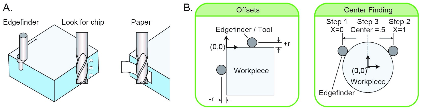
Fig 2. Techniques for aligning the tool in the x–y plane. (A) Illustrations of the (i) edgefinder, (ii) chip, and (iii) paper techniques. (B) Guide to offsetting a tool (left) and finding the center of an object (right).
(i) Edgefinder Technique
Tooling Note: This technique requires an edgefinder (e.g., #02035186, MSC Industrial Supply).
Step 1: Place edgefinder in collet and start spindle (1000 rpm works well with the edgefinder). Step 2: Deflect the tip of the edgefinder so that it lies eccentric to its initial axis. Step 3: Starting with the x-axis, move the edgefinder toward a perpendicular surface. The tip of the edgefinder will become concentric upon contact with surface, and then return to an eccentric position immediately afterward. This sudden “jump” in eccentricity marks the edge. Step 4: Set the current location to either plus or minus the radius of the tip. See Fig. 2B for more details on deciding a positive or negative bias.
Chip Technique
Tooling Note: This technique does not require any specific tooling.
Step 1: Start with the tool near the face of interest with the spindle running (i.e., the tool should be rotating). Step 2: Step the tool towards the surface, until (a) a chip is observed, (b) a mark is made on the surface, or (c) a sound is made from the tool cutting the material. Step 3: Set this location as (plus or minus) the radius of the endmill.
Tip: This method works best for large diameter endmills. Note that this is a physical contact method, and will blemish the surface.
Paper Technique
Tooling Note: This technique requires a small piece of paper of known thickness.
Step1: Start with the tool near the face of interest with the spindle running Step 2: Gripping gently with thumb and fore-finger, or by pressing it against the surface place a piece of paper between the tool and the surface. Step 3: Step the tool towards the surface until the tool pulls the paper. Step 4: Set this location as (plus or minus) the sum of the endmill radius and paper thickness.
Tip: This method works best for large endmills. Caution: Be sure to keep fingers clear of the cutting tool.
Micromilling is a highly efficient method for fabricating microfluidic devices directly in polymeric materials like thermoplastics. A recent review article highlights the use and relevance of micromilling in the field of microfluidics.1 While milling is most popular among machinists, the technique is becoming cheaper and more accessible to many others. Thus, there is a need for disseminating technical know-how for achieving quality micromilled parts. One common technical issue is ensuring flat work surfaces, and eliminating warping and bending of thin plastics during micromilling, which can lead to uneven milling and large errors in feature dimensions. Here we present a simple technique to achieve flat work surfaces – leveled to within 40 μin / in (.04 μm / mm)) – and properly secure thin plastic workpieces to minimize warping. Please refer to the review article by Guckenberger and co-workers for a primer on micromilling
What do I need?
Tools:
CNC mill (PCNC 770, Tormach)
3/8” set screw holder (#31820, Tormach)
Granite block (6” x 12” x 2” Grade AA, Standridge)
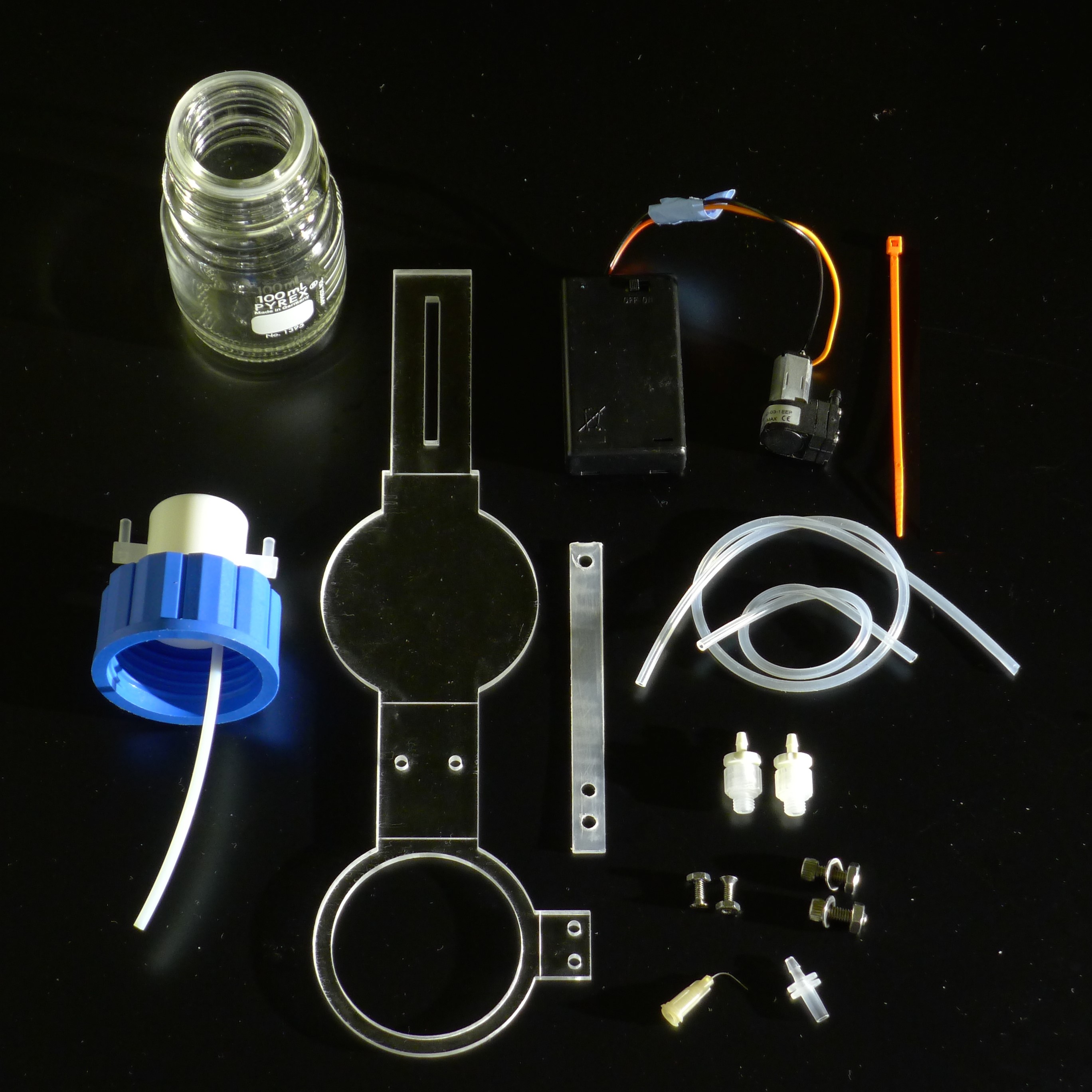
Fig. 1 Tooling and Materials. (A) Hardware necessary for setting up the granite block. Assembly of the T-slot clamps is shown in Fig. 2. (B)(Top) Components needed for the drop test indicator: (i) collet/tool holder, (ii) aluminum adapter, (iii) drop test indicator, (iv) screw to attach indicator to the adapter. (Bottom) Side view of the assembled components. (C) Materials needed for adhering workpiece to the block: (i) surface protection tape, (ii) silicone rubber, (iii) transfer tape, (iv) polystyrene sheet.
What do I do?
Preparation: The dial indicator must be affixed to the head of the mill. To do so, mounting brackets can be purchased or custom-made, as we have done using a block of aluminum. This aluminum serves as a simple adapter between the dial indicator and the collet.
Step 1: Place granite block on the milling table. Note that a stiff yet compliant material is necessary between the block and the milling table to allow for minor adjustments. The particle-board feet affixed to the granite block by the manufacturer (Standridge) are sufficient.
Step 2: Assemble the clamps (Fig. 2A), and position the clamps in either a 3-clamp (Fig. 2B) or 4-clamp (Fig. 2C) configuration. The front of the clamp (i.e., the portion that contacts the granite block) should be the same height as or lower than the rear of the clamp.
Step 3: Hand-tighten each clamp, then tighten an addition 1/8th turn using a wrench.
Step 4: Level the granite block by using the drop test indicator to measure the height across the entire block. The following steps are recommended:
a) Lower the indicator onto the center of the block.
b) Move the indicator along x-axis to the two ends of the block, and note the height of both ends.
c) Position the indicator on the high side of the block and tighten the clamps until the height matches the low side.
d) Repeat steps (b) and (c) for the y-axis.
e) Repeat steps (b) to (d) until the block is level to desired tolerance.
f) Tip: When using the 4-clamp configuration, clamps should be equally tightened in pairs to maintain levelness in the other direction.
Fig. 2 (A) T-slot clamp setup configuration. (B) Granite block configuration using three clamps. (C) Granite block configuration using four clamps.
Step 5: (Optional) Apply a protective adhesive film to the workpiece. This will simplify removal of the transfer tape from the workpiece (see Video).
a) Peel a piece of protective adhesive film from the roll of film.
b) Place a piece of silicone rubber on the roll of tape or other cylindrical roll.
c) Place the protective adhesive film on top of the silicone rubber with the adhesive side face up, assuring the tape is flat.
d) Roll the workpiece onto the piece of tape. The silicone rubber will provide compliance below the tape to prevent bubbles in the tape.
e) Press the tape down to make sure it is fully adhered to the workpiece.
Step 6: Apply 2-sided tape or transfer tape to the workpiece
Step 7: Stick the workpiece onto the granite block.
Step 8: (Optional)Use the drop test indicator again to ensure the workpiece is flat.
Martin A. Fisher School of Physics, Brandeis University, Waltham, Massachusetts 02454, United States
Why is this useful?
To achieve high resolution and high aspect ratio features in contact lithography it is necessary to have the photomask in direct contact with the photoresist during the exposure. This is impeded by the formation of edge beads on the edge of the wafer, which can measure multiples of the nominal resist thickness [1].
Dedicated spin coaters remove edge beads automatically just after spin coating. However, during soft baking, a new edge bead forms due to the coffee ring effect [2]. It is therefore recommended, especially for thicker resist films, to remove the edge bead not before, but after soft baking [3].
Edge bead removal is not critical on single layer devices. However, for multi level designs, edge bead removal can improve the feature resolution significantly. This is especially the case if the first layer of resist is thick and the second layer is thin.
This article presents the fabrication and use of a simple and inexpensive device to reliably remove edge beads by solvent spraying.
What do I need?
Materials:
100 ml round media storage bottle GL45
Diba Labware bottle cap Q series GL45 2 x 1/4 -28 ports with valves (00945Q-2V)
acrylic sheet, 12” x 6”, 3/16” thick
polyethylene sheet, 1/16 “ thick
3x AAA battery pack with on/off switch + batteries
polypropylene tube fitting, male Luer slip to barbed coupler, 3/32″ tube ID
Tools:
hot air gun (Aoyue 968a+)
laser cutter (40W/45W CO2 Hobby Laser by Full Spectrum Laser) or scroll saw, drill press and drill bits
soldering iron (Aoyue 968a+) and solder
What do I do?
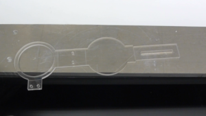
To build the edge bead remover, first prepare all components as shown in figure 1.
Cut the acrylic sheet and the polypropylene sheet and drill the holes as indicated in the schematic1.pdf or schematic1.dwg (AutoCAD) file. Solder battery pack wires to the pump. Then follow the instructions in video 1.
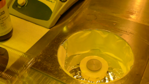
Center the wafer on spin coater and spin at 700 rpm. The optional centering tool used in the video was 3D printed on a formlabs form one 3D printer. (Use centering tool.stl file to reprint)
Turn on pump, open pump valve to pressurize bottle, position nozzle over edge bead.
Open spray valve and dissolve edge bead
Sweep outwards slowly and keep spraying for another 15 seconds.
Turn off spray valve and ramp up to 2000 rpm for 10 sec.
Turn off pump and close both valves. Developer may remain in the bottle and in the tubing.
Wafer does not have to be baked again and can be exposed immediately.
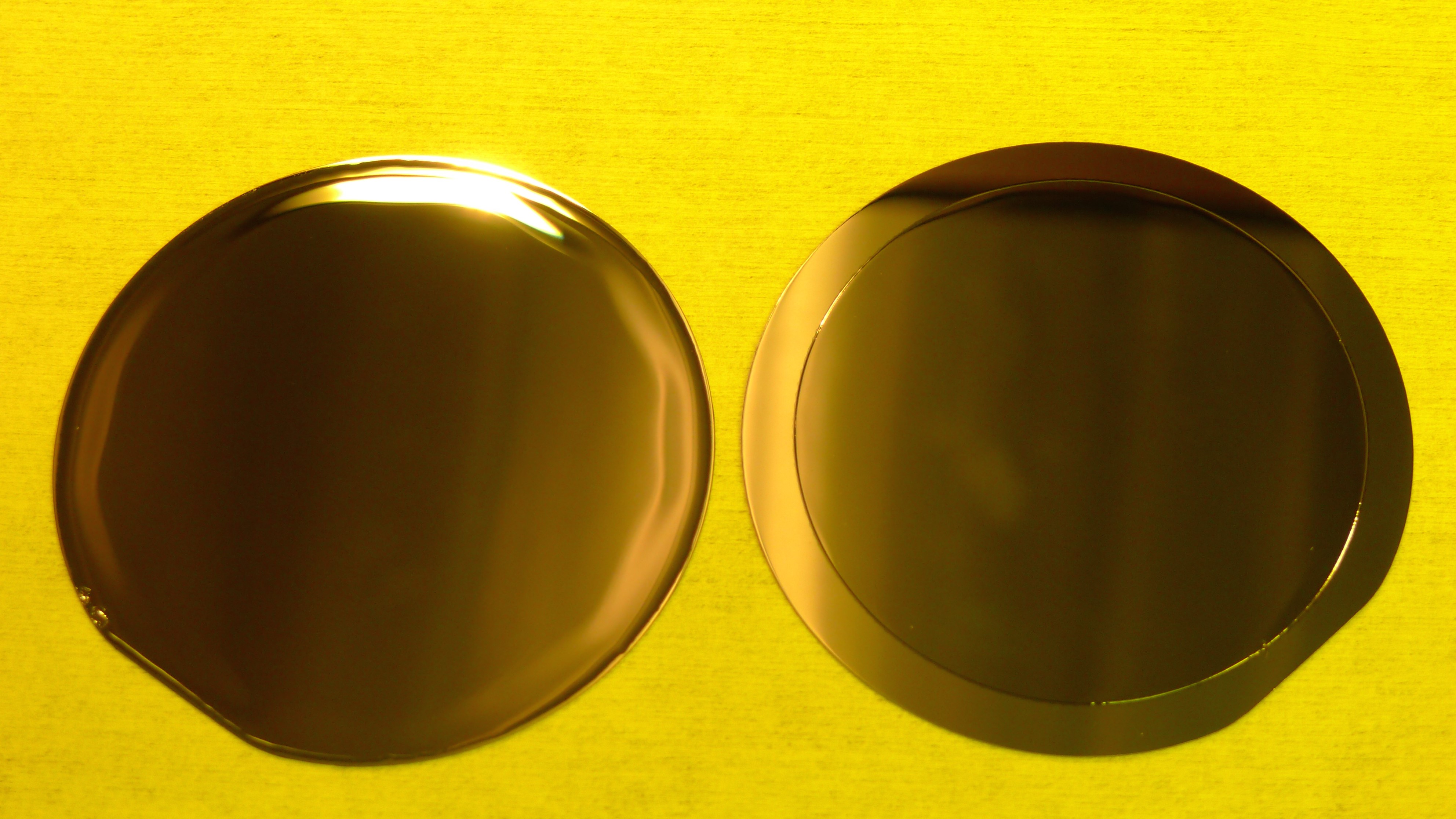
Figure 3: SU8 coated 3” wafer before (left) and after edge bead removal (right).
Figure 4: Comparison of feature resolution
CAD drawing of a multi layer design
Figure 5: SU8 master fabricated with edge bead
Figure 6: SU8 master fabricated without edge bead
Video 1:
Video 2:
References
[1] Shaurya Prakash, Junghoon Yeom, Nanofluidics and Microfluidics: Systems and Applications Micro and Nano Technologies, William Andrew, 2014
[2] Robert D. Deegan, Olgica Bakajin, Todd F. Dupont, Greb Huber, Sidney R. Nagel and Thomas A. Witten, Capillary flow as the cause of ring stains from dried liquid drops, Nature 389, 827-829 (23 October 1997), doi :10.1038/39827
Gabriele Pitingolo1, Raffaele Vecchione1,3 and Paolo A. Netti1,2,3
1Center for Advanced Biomaterials for Healthcare, Istituto Italiano di tecnologia (IIT@CRIB), Largo Barsanti e Matteucci, 53, 80125, Naples, Italy.
2 Dipartimento di Ingegneria Chimica, dei Materiali e della Produzione Industriale D.I.C.MA.P.I, Università di Napoli Federico II, Naples 80125, Italy.
3 Centro di Ricerca Interdipartimentale sui Biomateriali (CRIB), Università di Napoli Federico II, p.le Tecchio 80, Naples, 80125, Italy
Why is this useful?
Microfluidic chips are often made of silicon or glass which presents the drawbacks of being relatively expensive, time consuming and has limitations to the geometries that can be realized. PMMA is an optimal solution to overcome these aspects but it presents a low chemical resistance to organic solvents and aggressive chemicals
Norland Optical Adhesive 60 (“NOA60”) is a clear, colorless, liquid photopolymer that cures when exposed to ultraviolet light1. Surface bonding can be activated with light therefore monolithic and transparent devices especially useful for optical elements can be realized. In particular, the use of NOA 60 eliminates premixing, drying, or heat curing operations common to other optical adhesive systems. Curing time is a matter of minutes and is dependent upon the thickness applied and the energy of ultraviolet light available. Dupont and colleagues have recently developed a NOA microfluidic channel via a photolithography multistep method that presents a long time process2.
Here, we demonstrate the possibility to micromachine already cured NOA substrates by micromilling that is much easier and cheaper than photolithographic techniques for fabrication of microchannels or microstructures in general. In addition, by micromilling it is possible to easily drill and make open channels in NOA substrates if needed. Also, in the case of microstructures on the two layers to be bonded if one layer presents microstructures with feature sizes below 25 micron and one substrate with feature sizes above this value then it is possible to prepare one substrate by photolithographic techniques and the other substrate by micromilling with following bonding, saving time and money.
What do I need?
Fully cured PDMS mold
Norland Optical Adhesive 60
UV light (E-Series Ultraviolet Hand Lamps)
Micromachining machine
Oxygen plasma machine
Clamp
What do I do?
1. Pour liquid photopolymer NOA into a preformed PDMS mold covering the entire surface (figure 1A). After a few minutes to stabilize the liquid polymer put the PDMS mold under UV light for 30 minutes at a 365 nm wavelength (fig.1B).
2. After the curing time, NOA substrate is ready to use; to fabricate a microfluidic chip two NOA substrates are prepared. NOA substrates are replicated onto flat PDMS surfaces exploiting the flexibility of the PDMS mold as shown in figures 2A and 2B.
3. Take the NOA substrate and mill a channel and related inlet/outlet holes using a micromilling machine (Minitech CNC Mini-Mill) (fig. 3A-3B), the certified positioning accuracy of the three-axis are 12″ / 300mm in x-axis, 9″ / 228mm in y-axis, and 9″ / 228mm in z-axis. To minimize the experimental uncertainty, the NOA substrates preformed in point 2 are smoothed before milling.
4. Prepare the NOA channel (clean with water and dry with an absorbent cloth) and treat the channel and top layer by exposing to oxygen plasma for 60s, at a pressure less than 0.1 Torr and with a plasma power of 20 W (fig 4A). Clamp the two substrates and put the clamped channel under UV-light for 1 h finalizes the bonding process (fig 4B).
5. Your well-bonded NOA microfluidic chip (Figure 5) is now ready to use.
Luis G. Rigat-Brugarolas1,2, Antoni Homs-Corbera1,2 and Josep Samitier1,2,3
1 Nanobioengineering group, Institute for Bioengineering of Catalonia (IBEC), Barcelona, Spain 2 Centro de Investigación Biomédica en Red de Bioingeniería, Biomateriales y Nanomedicina (CIBER-BBN), Zaragoza, Spain.
3 Department of Electronics, Barcelona University (UB), Martí I Franques, 1, Barcelona, 08028, Spain.
Why is this useful?
At present, normal photolithographic techniques constitutes binary image transfer methodologies, where the developed pattern consists of regions with or without photoresist depending whether the UV Light has been in contact with the sample or not during the exposure process.1 Complex 3D patterns construction is of increasing importance in the miniaturization of fluidic devices.2 In the following work we introduce a photoresist-based technique to produce three-dimensional ramped microstructures for lab-on-a-chip applications.
We present a new technique that can be used to form multilevel features in SU-8 or any other negative photoresist using a single photolitograpy step, thus minimizing stages in the fabrication process in a simple and cheap way. This method thereby allows using a normal photomask without needing to add a complementary grayscale pattern, enabling complex microchannel structures.
What do I need?
Common items and devices used in photolitographic processes (mask aligner, hot plates, chemical baths, negative photoresist and transparent substrate)
Step Variable Metallic Neutral Density Filters (Thorlabs, Inc., NJ, USA).
What do I do?
Dispose the sample in the mask aligner with the SU-8 photoresist on the bottom side as depicted in Figure 1. This will force UV light to cross through the transparent substrate and to first polymerize those photoresist regions in contact with the substrate.
Place the photomask in the aligner standard position, normal to the light beam.
Select the filter (continuous, step, etc.) according to your needs (see an example in Figure 2).
Place the filter in the position between the photomask and the UV light source, with the filter’s design in contact with the photomask (see Figure 3).
Enter a correct UV exposure time; since another element is going to be added in the UV light trajectory, this value has to be adjusted (final result in Figure 4).
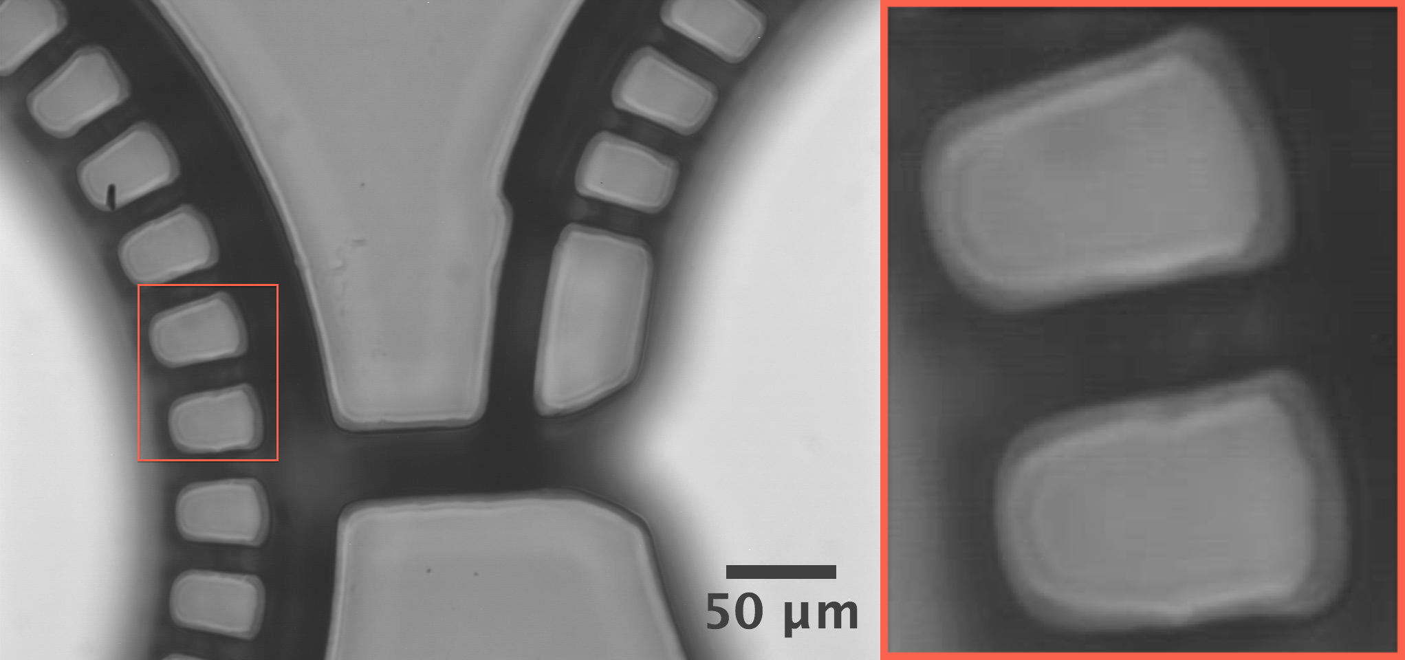
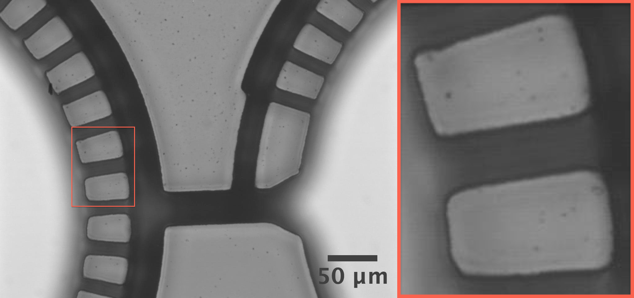
Fig 1: Scheme of disposal of the SU-8 photoresist in the mask aligner for achieving relief structures.
Fig 2: Example of rectangular step filter available at Thorlabs, Inc.
Fig 3: Step filter placed between the photomask and the UV light source.
Fig 4: Example of three-dimensional ramped structure constructed using SU-8. Relief characterization obtained with a profilometer. The white line represents the structure obtained after the development process (with an angle value of 30º), showing a slope from 0 µm to 12 µm (in this case, a rectangular step filter was used). The red line shows what it would look like the profile if no filter had been dispose between the photomask and the UV light source.
What else should I know?
As with any negative photoresist, grayscale exposure in conventional processes will lead to hardening the surface, removing the substrate if unattached during the development, in a methodology normally used to create cantilever structures. This is why it is important, when trying to create relief structures, to turn the sample and expose it from the glass substrate side leaving the SU-8 or any other negative photoresist on the bottom side.
Acknowledgments
We thank David Izquierdo and Juan Pablo Agusil for their technical help and for providing the material.
Reference
[1] S.D. Minteer. Microfluidic techniques: reviews and protocols. Humana Press, 2006. ISSN: 1064-3745.
[2] C. Chen, D. Hirdes, A. Folch. Gray-scale photolithography using microfluidic photomasks. PNAS, 2003. DOI:10.1073
Comments Off on Simple fabrication of three-dimensional ramped microstructures using SU-8 negative photoresist
Luis G. Rigat-Brugarolas1,2, Antoni Homs-Corbera1,2 and Josep Samitier1,2,3
1 Nanobioengineering group, Institute for Bioengineering of Catalonia (IBEC), Barcelona, Spain
2 Centro de Investigación Biomédica en Red de Bioingeniería, Biomateriales y Nanomedicina (CIBER-BBN), Zaragoza, Spain.
3 Department of Electronics, Barcelona University (UB), Martí I Franques, 1, Barcelona, 08028, Spain.
Why is this useful?
Nowadays it is common to fabricate multi-layered microfluidic microdevices by means of photolithographic techniques to create sophisticated structures allowing novel functionalities.1,2 Without any doubt, one of the critical steps in this manufacturing process is the alignment of the different transparent layers to perform the final device.
Several approaches have been made and studied to obtain a correct structuring of the three-dimensional device like, for example, the use of gold deposition, by means of sputtering techniques, for drawing the alignment marks in the substrate,3 or using expensive mask aligners with integrated alignment protocols. Those methods are expensive and laborious. In this work we present a novel, simple and non-time-consuming methodology for drawing alignment marks using Ordyl SY330 negative photofilm, a photoresist that can be easily displayed in the substrate and, thanks to its green color, it can be readily seen in a standard microscope.
What do I need?
Common items and devices used in photolithographic processes (mask aligner, hot plates and transparent substrate)
Sheets of Ordyl SY330 negative photofilm.
Ordyl Developer, SU-8 Developer or acetone.
Photomask with the alignment marks details.
Hot laminator.
What do I do?
A scheme of the alignment marks’ fabrication process can be seen in Figure 1. The steps are as follows:
Dispose the Ordyl photofim over the substrate (Figures 1A-B and 2).
Introduce both the substrate and the Ordyl film in a hot laminator in order to attach it firmly (see Figure 3).
For the exposure, use an acetate or chrome-on-glass photomask (an example can be seen in Figure 4) with the design of the alignment marks. Because Ordyl is a negative photoresist, the design should have the marks in transparent in order to polymerize them and draw them in the substrate (Figure 1C).
After exposure to UV Light (Figures 1D-E), an Ordyl Developer is needed (or, failing this, SU-8 developer or acetone), for having the final marks drawn in the substrate (an example can be seen in Figure 5).
Fig 1: Scheme of the fabrication process of the Ordyl alignment marks.
Fig 2: Placement of Ordyl photofilm on a microscope slide.
Fig 3: The hot laminator is used to attach the Ordyl film to the substrate.
Fig 4: Photomask with the design of the alignment marks.
Fig 5: Example of Ordyl alignment marks on a glass substrate.
Reference
[1] Dongeun Huh, Hyun Jung Kim, Jacob P Fraser, Daniel E Shea, Mohammed Khan, Anthony Bahinski, Geraldine A Hamilton and Donald E Ingber. Microfabrication of human organs-on-chips. Nature protocols. 2013 Nov. 11, vol.8. Doi:10.1038/nprot.2013.137.
[2] Michael P Cuchiara, Alicia CB Allen, Theodore M Chen, Jordan S Miller, Jennifer L West. Multilayer microfluidic PEGDA hydrogels. Biomaterials.2010 31 5491e5497
[3] Eugene JH Wee, Sakandar Rauf, Kevin MS Koo, Muhammad JA Shiddiky, and Matt Trau. µ-eLCR: A Microfabricated Device for Electrochemical Detection of DNA Base Changes in Breast Cancer Cell Lines. LabChip.2013 Nov 21;13(22):4385-91. DOI: 10.1039/c3lc50528f.
Comments Off on Simple alignment marks patterning for multilayered master fabrication
Previously we presented a method for connecting inlets and outlets to an external source that involved tubing and needles [1]. However, the process involves the use of needles which could be a safety concern. The process is also somewhat time-consuming. We have now developed a more convenient and rapid method for fabricating inlets/outlets in a PDMS chip without the need for needles.
What do I need?
A puncher, for example, we use a Schmidt punch press (Syneo, LLC)
Connectors with barbs and corresponding tubings, for example, we use elbow tube fitting with classic series barbs for 1/16” (1.6 mm) ID tubing (Valueplastic.com)
What do I do?
1. When the PDMS device has been cured, punch inlets and outlets from the top of the device.
(a)
(b)
(c)
Figure 1: (a) Schmidt Press; (b) punching through holes at desired locations on the device; (c) device with a set of three punched holes.
2. After sealing the device, insert the connectors (“Elbow Tube Fitting with classic series Barbs, 1/16”, (1.6 mm) ID Tubing, White Nylon”) into the inlets and outlet.
3.Tubing can then be connected to the connectors at one end, and to a syringe pump at the other end.
What else should I know?
The diameter of the punched holes is specific to the nominal cutting edge diameter of the punch. The punch, connectors, and tubing can be any size as long as they correspond to each other so that the connection does not leak. The connectors and tubing can be ordered from Value Plastics, INC.
The height of the Schmidt press can be adjusted according to the thickness of the PDMS device to ensure a through hole.
The maximum pressure we have tried with this type of connection is about 240 kPa, beyond which other parts of the chip fail (such as the PDMS/glass).
bonding.
Reference
[1] P. Li., W. Xue, and J. Xu, The fabrication of PDMS interconnecting interface assisted by tubing fixation, Lab Chip, Chips and Tips, 10 June 2011
Comments Off on Rapid fabrication of in/outlets for PDMS microfluidic devices
Gabriele Pitingolo, Enza Torino and Raffaele Vecchione Center for Advanced Biomaterials for Healthcare, Istituto Italiano di tecnologia (IIT@CRIB), Largo Barsanti e Matteucci, 53, 80125 – Napoli – Italy.
Why is this useful?
Common systems to connect microfluidics devices with classic fluidic equipment (such as syringe or peristaltic pumps) are based on the use of commercial connectors which are not always compatible with the device material.
Upchurch (Oak Harbor, WA, USA) NanoPorts™ assemblies are the first commercially available products to provide consistent fluid connectors for microfluidic chips. These products bond easily to some chip surfaces such as glass and polydimethylsiloxane (PDMS) with the provided preformed adhesive rings. All NanoPort™ components are made of inert, biocompatible PEEK™ polymer (nuts and ports) and Perlast® perfluoroelastomer (ferrules and gaskets). However, many microfluidic devices are made of polymethylmethacrilate (PMMA) and in this case the preformed adhesive rings are not suitable.
Here, we demonstrate an easy and effective way to bond NanoPorts to PMMA microdevices. Our approach is a hybrid system which glues the commercial nanoports with an alternative epoxy adhesive. Also remarkably this is a reusable system, in fact the Flat Bottom Port and the Flat Bottom Port Gasket may be removed and re bonded on another device as explained in the procedure.
What do I need?
Fully cured PMMA microchip with via holes to microchannels
UPCHURCH® SCIENTIFIC NanoPort Assemblies [1]
Loctite Super Attak Power Flex Gel (5g)
Binder Clip Medium 1-1/4in
FEP Tubing, 1/16’’ x 0.25 mm [2]
Scalpel and tweezers
Ethanol
Hammer
What do I do?
1. Prepare the PMMA surfaces (clean with water and dry with an absorbent cloth) and NanoPort™ for bonding (Figure 1). The Inlet and Outlet holes must be of a diameter below the inner diameter of the Nanoport (around 2 mm) to guarantee no leakage at the Nanoport-PMMA interface.
2. Put a few drops of Loctite Super Attak Flex Power Gel (5g) on a surface, in our case we used a piece of PMMA (Figure 2). Take the UPCHURCH® SCIENTIFIC NanoPort, insert the gasket seal into the recess in the bottom of the port (Figure 3) and touch the port to the drop of Loctite Super Attak in order to deposit the right amount of glue on the bonding surface (Figure 4). Eliminate the excess glue with the aid of a scalpel and attach the flat bottom port gasket directly on the bottom of the port (Figure 5).
3. Take the complete Nanoport (flat bottom port and gasket) and touch the drop of Loctite super attack, eliminating the excess glue with the aid of a scalpel. Center and place the complete Nanoport on your final substrate surrounding the access hole (Figure 6).
4. Clamp the port to the substrate (Figure 7) for 3 hours.
5. Your well-bonded NanoPort interconnect to PMMA (Figure 8) is now ready to use.
6. It is possible to remove the Nanoport from the PMMA surface. Use ethanol to weaken the epoxy (Figure 9) and after 30 minutes punch with a hammer to separate the NanoPort™ from the PMMA device.


")


