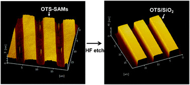
Contact area lithography has been used for directly patterning and transferring self-assembled monolayers (SAMs) onto silicon-based substrates.
Hyunjung Shin and colleagues from Kookmin University, in South Korea used a patterned (hard) silicon oxide template and placed it on substrates of interest, introducing a small amount of water in the process.
After drying off the water, the non-contacted areas served directly as growth sites of OTS-SAMs by simple solution deposition. The hard template was then detached from the substrate and the patterns of SAMs were obtained.
In principal, the hard template is cleansable by simple chemical etching without causing any damage. It is also 100% recyclable and can be reused up to ~50 times.
Fancy finding out more about this technique? Then why not download the communication today, which has been published in ChemComm and will be free to access until the 13th May 2011.


